


 It’s Only Common Sense: Create Passion That Customers Feel
 Punching Out: How to Stay Focused in Business and M&A
 Marcy’s Musings: Old School vs. New School—When Does It Matter?


The big construction cranes in Leoben Hinterberg have disappeared and the view is unobstructed again. It is now easy to see which milestones and records AT&S has achieved within a very short period of time – not just at the headquarters in Leoben. The research and development center with its series production for IC substrate technology is in itself a lighthouse project.
“Setting up this technology outside of Asia and bringing an IC substrate production facility of this dimension to the western world for the first time is a one-of-a kind project in and for Europe,” says project leader Nikolaus Bauer-Oeppinger and adds: “We are on schedule with the construction site and alongside the final exterior work, we started to move in the first production machines in April. Now there is nothing in the way of starting the qualification in the near future so that we can broaden our customer portfolio and supply our customers even faster and better.”
The building envelope of the future R&D and IC substrate center, which will open as plant 3 alongside the two existing production facilities in Leoben Hinterberg, was put up in a record time of only 14 months. A mighty bridge made of glass and steel connects the new competence center with the existing plants.
Largest construction site in Styria
The figures associated with the 500-million-euro project are impressive and make it the largest construction site in Styria: at the peak of the activities in March and April, 1,100 people were working on the building site and the delivery of machines. 11,000 sqm of clean room production area were established and the gross floor area amounts to 39,000 sqm – that equals six soccer fields for microelectronics. 80,000 tons of concrete and 4,700 tons of steel were used. Enough cables were laid to span the distance from Leoben to Zagreb (270 km). Especially IC substrates – which are essential for the leading-edge applications in microelectronics – will be produced in Leoben from 2024 onwards: that is a first for Europe. AT&S thus underlines its role as an innovation driver and technology pioneer.
New machines of a completely different dimension will be used for this purpose: the special machinery and equipment required for the product miniaturization of future IC substrates allow us to advance to (printed circuit board) substrate structures 10 times thinner than a human hair.
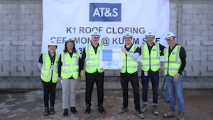
Two and a half Eiffel Towers in Kulim
Another two key milestones have been achieved at the even bigger AT&S Kulim site as the key executives of AT&S from Austria and Malaysia celebrated the roof closing of its first production plant and the installation of first set of tools. Production will start in autumn 2024. The second production plant has been paused at the status wind and water tight. The ramp-up depends on how the market develops.
At AT&S Kulim site, there are approximately 5,000 construction workers performing different construction tasks at site to deliver the fast track construction progress. Here, the figures are extremely impressive, too: The Kulim project will have a clean room area of 120,000 sqm – this corresponds to an incredible size of 17 soccer fields. The 24,000 tons of steel would be enough to build 2.5 Eiffel Towers.
AT&S’s Microelectronics Business Unit Executive Vice President Ingolf Schröder, comments: “I am tremendously delighted by the achievement of these two key milestones within 15 months after we broke the ground. They are victoriously accomplished after overcoming enormous health (pandemic), resources and logistical challenges.” AT&S’s Malaysia Managing Director Vittorio Villari, says: “The set-up of such a big plant has been achieved thanks to a pool of experienced talents and a matured electrical and electronics eco-system. AT&S collaborates with multinational corporations operating for more than 50 years in Malaysia, coupled with AT&S proprietary leading-edge high-end IC substrates technology.”
With the Austrian-based new production and research center of competence at the headquarters in Leoben, the new plant in Kulim and the strong and established production sites in Chongqing, Shanghai (both China), Ansan (Korea) and Nanjangud (India) AT&S is convinced to be ahead of the game. With cutting-edge technology, quality and excellence in PCBs and IC substrates AT&S is part of the solution for the future.


