


 Defense Speak Interpreted: Extreme Financial Disparity in Drones and Missiles
 American Made Advocacy: Five Years of Educating, Advocating, and Influencing Legislation and Policy
 The Right Approach: The End of an Era—DoD Proposes MIL-PRF-31032 Cancellation


Today, troops around the world can leverage troves of data at their fingertips, including at the tactical edge. That access marks an important step forward for warfighter technology, but to maximize decision-making at speed, these data volumes require granular, high-speed processing at their points of collection. High-performance computing relies heavily on internal microelectronics. Going forward, breakthrough performance will be driven by 3D heterogeneously integrated (3DHI) technologies that stack separately manufactured components, containing different semiconductors and materials, within a single package.
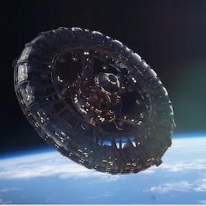
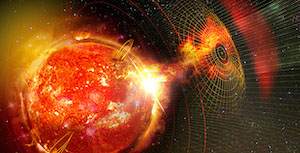
Critical applications will involve operating in extreme environments such as space, where components are subject to potentially destructive levels of radiation. With their multiple layers of vertically integrated circuits, complex interconnects, and diversity of materials, 3DHI components present new challenges for radiation testing and qualification.
The Advanced Sources for Single-event Effects Radiation Testing (ASSERT) program is focused on assuring that advanced U.S. microelectronics components can operate in harsh radiation environments with the highest-possible reliability. To facilitate the development of optimally radiation-hardened (rad-hard) components – and to rapidly deliver cutting-edge tech to the warfighter – ASSERT seeks to disrupt the status quo in rad-hard design and qualification by integrating radiation testing throughout the design and development lifecycle.
The space domain’s continued growth affects both U.S. national security and economic interests. ASSERT aims to accelerate the availability of radiation-qualified, state-of-the-art components 10 times faster when compared with current approaches.
“Today it takes on the order of five to 10 years to design, fully qualify, and deploy a rad-hard part. If you think about processors from 10 years ago, they are at least four orders of magnitude behind modern computing performance,” said Dr. David K. Abe, ASSERT program manager. “To speed the time to deployment, the goal is to make radiation testing an integral part of the design, fabrication, and development processes, instead of waiting until the end to do the final testing.”
By developing sources to achieve integration of testing at the factory and lab levels, ASSERT will enable teams to iteratively improve component design and resilience. This is especially significant given emerging technologies, evolving operational conditions, and the long lead times to access the few specialized facilities capable of the heavy-ion testing required to test electronics for high radiation environments.
“This isn’t just about testing; it’s about enabling the warfighter. In terms of the processing and reliability of space-based assets, the disparity is tremendous between what’s available and qualified today and where we need to be. With ASSERT, we’re working to close that gap,” Abe said. “We’ll be able to put advanced electronics into space and onto strategic platforms much faster than we can today – that’s the mission requirement.”


