


 The Hidden Enabler of Autonomous Warfare: Advanced PCB Technologies Behind Defense AI
 It’s Only Common Sense: Stay Curious, My Friends


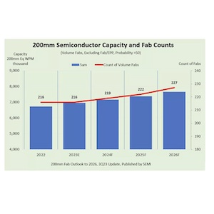
Semiconductor manufacturers worldwide are projected to increase 200mm fab capacity by 14% from 2023 through 2026, adding 12 new 200mm volume fabs (excluding EPI) as the industry reaches a record high of more than 7.7 million wafers per month (wpm), SEMI announced in its 200mm Fab Outlook to 2026 report.
LogoPower and compound semiconductors, which are vital for the consumer, automotive and industrial sectors, are the biggest drivers of 200mm investment. The development of powertrain inverters and charging stations for electric vehicles (EVs) in particular is expected to fuel increases in global 200mm wafer capacity as EV adoption continues to rise.
“The global semiconductor industry’s ramp to record 200mm fab capacity highlights the bullish expectations for growth in the automotive market in particular,” said Ajit Manocha, SEMI President and CEO. “While automotive chip supply has stabilized, the increased chip content in EVs and the drive to reduce charging time is spurring capacity expansions.”
Chip suppliers including Bosch, Fuji Electric, Infineon, Mitsubishi, Onsemi, Rohm, STMicroelectronics and Wolfspeed are accelerating their 200mm capacity projects to meet future demand.
The SEMI 200mm Fab Outlook to 2026 report shows fab capacity for automotive and power semiconductors growing 34% from 2023 to 2026, with Microprocessor Unit/Microcontroller Unit (MPU/MCU) ranking second at 21%, followed by MEMS, Analog, and Foundry at 16%, 8%, and 8%, respectively.
Accounting for most of the 200mm fab capacity are 80nm to 350nm technology nodes. Growth of 80nm to 130nm node capacity is forecast to expand by 10%, while 131nm to 350nm technology nodes are expected to register an 18% expansion from 2023 to 2026.
Regional Outlooks
Southeast Asia is projected to lead 200mm capacity growth with a 32% increase during the report period. China is expected to rank second with 22% growth. The biggest contributor to the 200mm capacity expansion, China is projected to reach more than 1.7 million wafers per month by 2026. Americas, Europe & Mideast, and Taiwan will follow at 14%, 11%, and 7% growth, respectively.
In 2023, China is forecast to claim 22% share of 200mm fab capacity, while Japan is expected to account for 16% of total capacity, followed by Taiwan, Europe & Mideast, and America at 15%, 14%, and 14%, respectively.


