-
- News
- Books
Featured Books
- pcb007 Magazine
Latest Issues
Current IssueAdvancing the Advanced Materials Discussion
Moore’s Law is no more, and the advanced material solutions to grapple with this reality are surprising, stunning, and perhaps a bit daunting. Buckle up for a dive into advanced materials and a glimpse into the next chapters of electronics manufacturing.
Inventing the Future With SEL
Two years after launching its state-of-the-art PCB facility, SEL shares lessons in vision, execution, and innovation, plus insights from industry icons and technology leaders shaping the future of PCB fabrication.
Sales: From Pitch to PO
From the first cold call to finally receiving that first purchase order, the July PCB007 Magazine breaks down some critical parts of the sales stack. To up your sales game, read on!
- Articles
- Columns
- Links
- Media kit
||| MENU - pcb007 Magazine
AT&S Establishes the Cleanest Working Environment in Styria
November 24, 2023 | AT&SEstimated reading time: 2 minutes

As a globally active high-tech group and a key driver of technological development in microelectronics, AT&S is currently completing its “lighthouse project” in Leoben-Hinterberg. The new R&D center for IC substrates and packaging technologies is a unique development and production center for connection technologies and substrates in the high-end technology sector in the western world. It will start production in 2024.
300 new jobs
The leading market position that AT&S has built up over the past decades allows the Leoben-based high-tech company to continue to grow. “We need bright minds and skilled hands for our future tasks,” says Eduard Lackner, Senior Manager HR for Austria at AT&S. The new competence center in Leoben will create a total of 700 new jobs. 270 new employees have already been brought on board, and the intensive search is now underway for a further 300 specialists.
300 new jobs have been advertised as operators in the production and manufacturing areas, in the laboratory (chemistry), in maintenance as well as positions aimed at HTL graduates as a first career opportunity. In general, basic technical training (such as electrical engineering, mechanical engineering, mechatronics or industrial installation), manual skills and reliability are required.
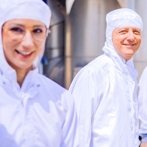
The cleanest workplace in Styria
This new R&D center with substrate production is an end-to-end clean room construction. With the ISO 3 and ISO 4 cleanrooms (or cleanroom 1000 and cleanroom 10,000) required for substrate production, these workplaces are cleaner than a hospital’s surgery room, as even the smallest particles of dirt and contamination such as hair or make-up residue endanger the high-tech products. It is therefore fair to say that AT&S has established the cleanest working environment in Styria.
Reduced working hours, 300 euro shift bonus
What makes the jobs even more attractive is the five-shift operation and a fixed sequence of morning, afternoon and night shifts. The average annual working time is reduced to 32.4 hours per week. The remuneration models are enhanced with a shift bonus of 300 euros. “Even those who have previously worked in non-technical areas can apply for these positions at AT&S,” says Eduard Lackner. “We have training programs and also make career changers fit for our high-tech world.” English is established as the corporate language in the multinational working environment at AT&S, but it is not a prerequisite for the production areas. “Production will start at the new center at the beginning of 2024, and we want to have as many new employees on board as possible for this intensive phase.”
Testimonial
"Our marketing partnership with I-Connect007 is already delivering. Just a day after our press release went live, we received a direct inquiry about our updated products!"
Rachael Temple - AlltematedSuggested Items
Knocking Down the Bone Pile: Best Practices for Electronic Component Salvaging
09/17/2025 | Nash Bell -- Column: Knocking Down the Bone PileElectronic component salvaging is the practice of recovering high-value devices from PCBs taken from obsolete or superseded electronic products. These components can be reused in new assemblies, reducing dependence on newly purchased parts that may be costly or subject to long lead times.
On the Line With… Podcast: UHDI and RF Performance
09/17/2025 | I-Connect007I-Connect007 is excited to announce the release of a new episode in its latest On the Line with... podcast series, which shines a spotlight on one of the most important emerging innovations in electronics manufacturing: Ultra-High-Density Interconnect (UHDI).
The Marketing Minute: Cracking the Code of Technical Marketing
09/17/2025 | Brittany Martin -- Column: The Marketing MinuteMarketing is never a one-size-fits-all endeavor, but the challenges are magnified for highly technical industries like electronics. Products and processes are complex, audiences are diverse, and the stakes are high, especially when your customers are engineers, decision-makers, and global partners who depend on your expertise.
EV Group Achieves Breakthrough in Hybrid Bonding Overlay Control for Chiplet Integration
09/12/2025 | EV GroupEV Group (EVG), a leading provider of innovative process solutions and expertise serving leading-edge and future semiconductor designs and chip integration schemes, today unveiled the EVG®40 D2W—the first dedicated die-to-wafer overlay metrology platform to deliver 100 percent die overlay measurement on 300-mm wafers at high precision and speeds needed for production environments. With up to 15X higher throughput than EVG’s industry benchmark EVG®40 NT2 system designed for hybrid wafer bonding metrology, the new EVG40 D2W enables chipmakers to verify die placement accuracy and take rapid corrective action, improving process control and yield in high-volume manufacturing (HVM).
ROHM Develops Ultra-Compact CMOS Op Amp: Delivering Industry-Leading Ultra-Low Circuit Current
09/11/2025 | ROHMROHM’s ultra-compact CMOS Operational Amplifier (op amp) TLR1901GXZ achieves the industry’s lowest operating circuit current.