


 It’s Only Common Sense: Customers Capabilities—and Confidence
 Dan’s Biz Bookshelf: ‘The 'NVIDIA Way: Jensen Huang and the Making of a Tech Giant’


Intel Opens Fab 9 in New Mexico
January 25, 2024 | IntelEstimated reading time: 2 minutes
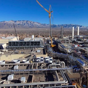
Intel celebrated the opening of Fab 9, its cutting-edge factory in Rio Rancho, New Mexico. The milestone is part of Intel's previously announced $3.5 billion investment to equip its New Mexico operations for the manufacturing of advanced semiconductor packaging technologies, including Intel’s breakthrough 3D packaging technology, Foveros, which offers flexible options for combining multiple chips that are optimized for power, performance and cost.
“Today, we celebrate the opening of Intel’s first high-volume semiconductor operations and the only U.S. factory producing the world’s most advanced packaging solutions at scale. This cutting-edge technology sets Intel apart and gives our customers real advantages in performance, form factor and flexibility in design applications, all within a resilient supply chain. Congratulations to the New Mexico team, the entire Intel family, our suppliers, and contractor partners who collaborate and relentlessly push the boundaries of packaging innovation,” said Keyvan Esfarjani, Intel executive vice president and chief global operations officer.
Intel’s global factory network is a competitive advantage that enables product optimization, improved economies of scale and supply chain resilience. The Fab 9 and Fab 11x facilities in Rio Rancho represent the first operational site for mass production of Intel’s 3D advanced packaging technology. It is also Intel's first co-located high-volume advanced packaging site, marking an end-to-end manufacturing process that creates a more efficient supply chain from demand to final product.
Fab 9 will help fuel the next era of Intel’s innovation in advanced packaging technologies. As the semiconductor industry moves into the heterogeneous era that uses multiple “chiplets” in a package, advanced packaging technologies, such as Foveros and EMIB (embedded multi-die interconnect bridge), offer a faster and more cost-efficient path toward achieving 1 trillion transistors on a chip and extending Moore’s Law beyond 2030.
Foveros, Intel’s 3D advanced packaging technology, is a first-of-its-kind solution that enables the building of processors with compute tiles stacked vertically, rather than side-by-side. It also allows Intel and foundry customers to mix and match compute tiles to optimize cost and power efficiency.
"This investment by Intel underscores New Mexico’s continued dedication to bring manufacturing back home to America," said Gov. Michelle Lujan Grisham. "Intel continues to play a key role in the state’s technology landscape and strengthen our workforce, supporting thousands of New Mexico families.”
The $3.5 billion investment in Rio Rancho has created hundreds of high-tech Intel jobs, more than 3,000 construction jobs and an additional 3,500 jobs across the state.
Share on:


Testimonial
"In a year when every marketing dollar mattered, I chose to keep I-Connect007 in our 2025 plan. Their commitment to high-quality, insightful content aligns with Koh Young’s values and helps readers navigate a changing industry. "
Brent Fischthal - Koh YoungSuggested Items
Webinar Review, Part 2: Building the AI Backbone at IBM on Systems-level Packaging
04/20/2026 | Marcy LaRont, I-Connect007The second presentation in a recent Global Electronics Association’s Executive Pulse webinar series widened the lens on advanced packaging, moving beyond the component level to a systems-level view of how AI is reshaping the electronics landscape. Building on Dr. Hemanth Dhavaleswarupu of AMD’s previous discussion of chip-level packaging innovation, Dr. Jung Yoon of IBM explored the broader infrastructure implications, from the data center floor to the global supply chain.
Applications, Challenges, and the Future of Flex–Packaging Integration, Part 2
04/16/2026 | Anaya Vardya, American Standard CircuitsIn the second of this two-part series, Anaya Vardya of American Standard Circuits examines applications, challenges, manufacturing considerations, and future trends emerging from the convergence of flexible printed circuit boards and advanced semiconductor packaging. Applications driving the convergence include consumer electronics, automotive systems, medical, wearables, aerospace and more.
From AI to AEP, an Impressive Array of Keynotes at APEX EXPO 2026
04/17/2026 | Marcy LaRont and Nolan Johnson, I-Connect007Each year at APEX EXPO, the Global Electronics Association provides an impressive lineup of keynote speakers to kick off the largest electronics manufacturing event in North America. This year included four keynote speeches, on topics ranging from the promise and peril of AI to the power of electronics, quantum computing, and the importance of heterogeneous integration in advanced electronics packaging.
AI, Connectivity, and Systems-Level Thinking: New Frontiers in Advanced Packaging
04/16/2026 | I-Connect007 Editorial TeamThe upcoming issue of Advanced Electronics Packaging Digest examines key developments shaping the next phase of electronics innovation, from the reliability challenges of AI-driven packaging to emerging connectivity standards and the broader systems-level implications of artificial intelligence.
Indium Showcases Solder Alloy Reliability Research for Heterogeneous Integration at ICEP-HBS
04/15/2026 | Indium CorporationIndium Corporation Senior Global Product Manager, Semiconductor and Advanced Materials, Sze Pei Lim will present a collaborative International Electronics Manufacturing Initiative (INEMI) project comparing SnBi and SAC305 solder alloys for first-level interconnects in complex heterogeneous packages.