


 Trouble in Your Tank: Implementing Direct Metallization in Advanced Substrate Packaging
 It’s Only Common Sense: Storytelling That Sells—Stop Pitching, Start Painting Pictures
 The Right Approach: Get Ready for ISO 9001 Version 6


Hitachi High-Tech Launches High-sensitivity and High-throughput Wafer Surface Inspection System LS9300AD for Wafer Manufacturers
March 15, 2024 | ACN NewswireEstimated reading time: 1 minute
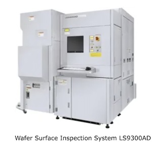
Hitachi High-Tech Corporation announced the launch of the LS9300AD, a new system for inspecting the front and backside of non-patterned wafer surfaces for particles and defects. In addition to the conventional dark-field laser scattering detection of foreign material and defects, the LS9300AD is equipped with a new DIC (Differential Interference Contrast) inspection function that enables detection of irregular defects, even shallow, low aspect microscopic defects. LS9300AD has the wafer edge grip method and rotating stage currently used in conventional products to enabling front and backside wafer inspection.With the introduction of LS9300AD, Hitachi High-Tech enables reduced inspection costs and improved yield for semiconductor wafers and semiconductor device manufacturers by providing high-sensitivity and high-throughput detection of low-aspect microscopic defects.
Inspection of non-patterned semiconductor wafers' (before circuit pattern formation) surfaces and backside surfaces has been used in quality assurance during wafers shipment and acceptance, as well as for particles control in various semiconductor device manufacturing processes.Semiconductor wafers manufacturers, use it for quality control to inspect defects and particles that occur during the wafer manufacturing process. In recent years, semiconductor devices have become smaller and more complex, so the size of defects and foreign matter that affect yield in the semiconductor device manufacturing process has become smaller. Due to this, the need for managing all types of defects, including low-aspect microscopic defects on the surface and backside of wafers, is increasing. Responding to the changes in the social environment semiconductor production is expected to increase. To control inspection costs, high-sensitivity and high-throughput inspection equipment is required.
Share on:


Testimonial
"We’re proud to call I-Connect007 a trusted partner. Their innovative approach and industry insight made our podcast collaboration a success by connecting us with the right audience and delivering real results."
Julia McCaffrey - NCAB GroupSuggested Items
Preventing Surface Prep Defects and Ensuring Reliability
06/10/2025 | Marcy LaRont, PCB007 MagazineIn printed circuit board (PCB) fabrication, surface preparation is a critical process that ensures strong adhesion, reliable plating, and long-term product performance. Without proper surface treatment, manufacturers may encounter defects such as delamination, poor solder mask adhesion, and plating failures. This article examines key surface preparation techniques, common defects resulting from improper processes, and real-world case studies that illustrate best practices.
I-Connect007 Editor’s Choice: Five Must-Reads for the Week
06/06/2025 | Nolan Johnson, I-Connect007Maybe you’ve noticed that I’ve been taking to social media lately to about my five must-reads of the week. It’s just another way we’re sharing our curated content with you. I pay special attention to what’s happening in our industry, and I can help you know what’s most important to read about each week. Follow me (and I-Connect007) on LinkedIn to see these and other updates.
The Chemical Connection: Reducing Defects in Circuit Board Production
06/04/2025 | Don Ball -- Column: The Chemical ConnectionWe all agree that in any manufacturing process, reducing defects in your product induced during manufacture (aka increasing yields) is a good thing. Doing so, however, can be a source of contention and frustration. I don’t pretend to be an expert in this field, because most of my work involves feasibility studies for new concepts or testing improvements made to existing equipment. High yields were usually not a factor; it’s simply about having enough data to prove or disprove a concept or seeing whether improvements to equipment design actually work. However, here are some observations I made visiting quality shops where high production at high yields was important.
Smart Automation: AI—Revolutionizing Inspection in Electronics Manufacturing
05/27/2025 | Josh Casper -- Column: Smart AutomationArtificial Intelligence (AI) is rapidly becoming a staple in our personal and professional lives. In electronics manufacturing, integrating AI to combat common inefficiencies and to contextualize data will open new doors into how we supplement our traditional processes. In some specific areas of the electronics manufacturing process, integration of AI on the factory floor is already having a tremendous effect. One such area is PCBA inspection, particularly 3D automated optical inspection (AOI) systems.
Marcy’s Musings: The Relentless Pursuit of Perfection
05/16/2025 | Marcy LaRont -- Column: Marcy's MusingsFew things in this world are or will ever be perfect. For me, perfection might look like the vivid colors that only Mother Nature can create, the birth of a child, and the inner workings of the human brain. But all else in this physical, tangible world is, in one way or another, inherently flawed. Even the “flawless” diamond is more about the sheer awe and beauty of beholding near-perfection than perfection itself. In many ways, this truth provides great texture and diversity to our world. Yet, we still strive for perfection, and it’s in this that we learn and achieve higher heights than we otherwise would have.