


 Beyond the Board: The Future of Innovation—Why the Electronics Industry Needs You
 American Made Advocacy: New Congress, New Opportunities
 The Government Circuit: News on Defense Electronics, Europe, and Sustainability


Cost-optimize Your PCB Design and Specifications
August 20, 2024 | Erik Pedersen and Richard Koensgen, ICAPE GroupEstimated reading time: 1 minute
Knowledge is the key to identifying the small details that makes the big cost difference for your printed circuit board. There are many types of printed circuit boards and multiple choices between the development of schematic and BOM to PCB technology selection, electronic PCB design, mechanical and physical properties, and PCB specification.
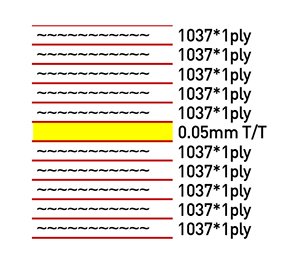
Component Technology and BGA Size
The component size and technology have the most significant influence on the PCB cost. Most surface-mounted microchips can be designed into standard PCBs with plated through-holes. If the same microchip comes in a BGA package, it might need microvias and buried vias using a higher wiring density to be designed into an HDI PCB. Generally, PCBs containing BGAs become HDI PCBs when the ball center-to-center pitch is below 0.8 mm. If your physical board properties allow it and the component availability is equal, you should strive to find the BGA with the largest pitch to reduce the component and PCB cost.
For example, the same BGA microchip can be found with pitch 0.8 mm, 0.6 mm, and 0.5 mm. The 0.8 mm pitch BGA can be routed on an eight-layer standard PCB with a price index of 100. The 0.6 mm pitch can be routed on a (1-6-1) eight-layer, one-step HDI PCB with a price index of 200. The 0.5 mm pitch BGA can be routed on a (2-4B-2) eight-layer, three-step HDI PCB with a price index of 350. The number of lamination steps is the most significant cost driver for HDI and ultra HDI PCBs. Designs with BGAs equal to or less than 0.4 mm and multiple rows challenge the capability of HDI suppliers, which leads to the use of UHDI design parameters and thereby reduces the availability and increases the cost.
Material Selection
Correct material selection that complies with the performance and functionality of your application also plays a crucial role in the PCB cost.
The most common stackups of standard PCBs are specified with 35 µm Cu on all layers. The manufacturer starts on 17.5 µm Cu on outer layers and 35 µm Cu on inner layers, since the final outer layer Cu thickness reaches approximately 35 µm after plating. But 35 µm Cu on the inner layers isn’t always required and can be replaced by 17.5 µm for the current flowing in many electronic devices. This, in turn, lowers costs.
To continue reading this article, which originally published in the August 2024 Design007 Magazine, click here.
Share on:


Suggested Items
Technica USA Showcases PCBA Supply Partners at IPC APEX EXPO 2025
03/13/2025 | Technica USATechnica USA is thrilled to highlight its full portfolio of PCBA supply partners at the 2025 APEX/IPC Expo in Anaheim, California. Featuring some of the world’s leading suppliers, Technica’s PCBA product lineup continues to drive innovation and excellence in the industry.
Aismalibar to Showcase Advanced Thermal Management Solutions at APEC 2025
03/13/2025 | AismalibarAismalibar, a global leader in high-performance thermal management materials, is set to exhibit at APEC 2025 (Applied Power Electronics Conference) in Atlanta, Georgia, from March 16–20, 2025. As the premier event for power electronics professionals, APEC provides a crucial platform for industry leaders to explore the latest advancements in thermal interface materials (TIMs), high-performance PCB laminates, and insulated metal substrates (IMS).
Technica USA Celebrates 40 Years of Excellence in Electronics Manufacturing
03/13/2025 | Technica USATechnica USA, a leading provider of materials, equipment, installation, and services for the printed circuit board (PCB) fabrication, PCB Assembly, substrates, MEMS, and semiconductor industries, proudly announces its 40th anniversary in 2025.
Elementary Mr. Watson: Ensuring a Smooth Handoff From PCB Design to Fabrication
03/13/2025 | John Watson -- Column: Elementary, Mr. WatsonAt the 2020 Tokyo Summer Olympics, the U.S. men's 4x100-meter relay team had high hopes of winning a medal. The team comprised some of the fastest sprinters in the world, but something went wrong. In a relay, four runners must smoothly pass their baton to the next runner inside a zone on the track. If a runner drops the baton or it’s passed outside the zone, the team risks disqualification. The U.S. team’s pass between the second and third runner was messy, slowing them down. By the time the last runner received the baton, the team had lost too much time. They finished sixth in their heat and didn’t qualify for the final.
MicroCraft to Unveil Three New Models at IPC APEX EXPO 2025
03/12/2025 | MicroCraftMicroCraft, a global leader in PCB testing and precision inkjet printing solutions, is set to showcase three cutting-edge models at IPC APEX EXPO 2025 at the Anaheim Convention Center March 18-20 in booth #4105. Each model represents the latest advancements in speed, accuracy, and automation across MicroCraft’s three product lines.