


 The Knowledge Base: A Conference for Cleaning and Coating of Mission-critical Electronics
 Defense Speak Interpreted: Is DARPA Still Around After CHIPS?
 Beyond the Board: Orbital High Ground—Why Space Superiority Is Slipping Away


Effects of Advanced Packaging and Stackup Design
December 26, 2024 | I-Connect007 Editorial TeamEstimated reading time: 1 minute

Kris Moyer teaches several PCB design classes for IPC and Sacramento State, including advanced PCB design. His advanced design classes take on some really interesting topics, including the impact of a designer’s choice of advanced packaging upon the design of the layer stackup.
Kris shares his thoughts on the relationship between packaging and stackup, what PCB designers need to know, and why he believes, “The rules we used to live by are no longer valid.”
Kris, tell us how advanced packaging can impact stackup design. What challenges do designers need to be aware of?
Kris Moyer: With advanced packaging you usually need to use HDI or UHDI technology. This usually means sequential lamination. With sequential lamination you need to select materials that can survive multiple lamination thermal cycles.
When we were discussing advanced packaging and stackup design recently, you said, “The rules we used to live by are no longer valid.” Expand on that a little bit.
As I mentioned, your selection of materials is now further restricted by the need for materials that survive multiple lamination cycles. Additionally, since we are adding layers one at a time and need plating on all layers, not just the outer layers, the copper design is now more difficult. Also, since we are adding layers one at a time, we can now have some select instances of unbalanced Z-axis and still meet bow and twist. Furthermore, many of the ultra-thin dielectric layers used in HDI/UHDI are just resin-coated copper without any reinforcement, so CTE/FA can be more of an issue.
To read this entire conversation, which appeared in the December 2024 issue of Design007 Magazine, click here.
Share on:


Suggested Items
Meet the Author Podcast: Martyn Gaudion Unpacks the Secrets of High-Speed PCB Design
07/10/2025 | I-Connect007In this special Meet the Author episode of the On the Line with… podcast, Nolan Johnson sits down with Martyn Gaudion, signal integrity expert, managing director of Polar Instruments, and three-time author in I-Connect007’s popular The Printed Circuit Designer’s Guide to... series.
Showing Some Constraint: Design007 Magazine July 2025
07/10/2025 | I-Connect007 Editorial TeamA robust design constraint strategy balances dozens of electrical and manufacturing trade-offs. This month, we focus on design constraints—the requirements, challenges, and best practices for setting up the right constraint strategy.
Elementary, Mr. Watson: Rein in Your Design Constraints
07/10/2025 | John Watson -- Column: Elementary, Mr. WatsonI remember the long hours spent at the light table, carefully laying down black tape to shape each trace, cutting and aligning pads with surgical precision on sheets of Mylar. I often went home with nicks on my fingers from the X-Acto knives and bits of tape all over me. It was as much an art form as it was an engineering task—tactile and methodical, requiring the patience of a sculptor. A lot has changed in PCB design over the years.
TTCI Joins Printed Circuit Engineering Association to Strengthen Design-to-Test Collaboration and Workforce Development
07/09/2025 | The Test Connection Inc.The Test Connection Inc. (TTCI), a leading provider of electronic test and manufacturing solutions, is proud to announce its membership in the Printed Circuit Engineering Association (PCEA), further expanding the company’s efforts to support cross-functional collaboration, industry standards, and technical education in the printed circuit design and manufacturing community.
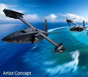
Bell to Build X-Plane for Phase 2 of DARPA Speed and Runway Independent Technologies (SPRINT) X-Plane Program
07/09/2025 | Bell Textron Inc.Bell Textron Inc., a Textron Inc. company, has been down-selected for Phase 2 of Defense Advanced Research Projects Agency (DARPA) Speed and Runway Independent Technologies (SPRINT) X-Plane program with the objective to complete design, construction, ground testing and certification of an X-plane demonstrator.