


 Trouble in Your Tank: At 40 GHz, Everything Matters, Part 2
 It’s Only Common Sense: Stop Watching the Headlines and Start Watching the Opportunity
 The Right Approach: The Pros and Cons of PCB Vertical Integration


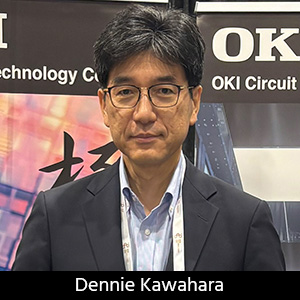
During PCB East, OKI Circuit Technology unveiled its latest innovation: a 124-layer printed circuit board that is 7.6 mm thick, marking a significant advancement in PCB technology. In this interview, “Dennie” Kazuo Kawahara, president of OKI Data Americas, and Eiichi Aki, sales and marketing specialist at OKI Circuit Technology, shared their insights into this feat. With plans for mass production starting in October, this board is designed for high-bandwidth memory applications, accommodating the demanding requirements of AI chips.
Andy Shaughnessy: Dennie, why don't you give us a little background on OKI, and then we’ll focus on this 124-layer circuit board.
Dennie Kawahara: OKI was established in 1881. We have evolved into many different business sectors. OKI is probably more known as a printer company in the U.S., but OKI in Japan is known for much more than printers. We have many different business sectors, and PCB is a main focus for the U.S. market—not just in the U.S. but globally. We exhibit at PCB East and PCB West every year. We just announced our 124-layer PCB just before this show.
Shaughnessy: I don't think I've ever heard of a 124-layer board before.
Kawahara: I'm sure there are companies that make them for specific applications, but I think we're the first one to make a broad announcement that this is our capability now.
Shaughnessy: This is not just a one-off board, right? This is full production?
Kawahara: Correct. We will have mass production capability starting in October. We made the first board, and we want to make sure that it is being distributed to everyone interested. Then, we can go full swing in October.
Shaughnessy: Is this something that traditional manufacturing can do, not requiring fancy buildup or additive processing or anything like that?
Eiichi Aki: This fabrication is simple, with a one-time lamination and flip-drilling, smooth from top to bottom. At that point, it’s just a conventional process.
Shaughnessy: Before that, you all had built a 108-layer board, which is still a pretty big board. This is a high-bandwidth memory testing board?
Aki: Yes, this time. It includes some HBM chips. They require a huge number of electrical connections in the circuit.
Shaughnessy: After fabricating a 124-layer printed circuit board, will you be aiming for even higher layer counts?
Aki: We are targeting a little higher, 130 layers or so. PCB manufacturing has a thickness limitation of about 300 mils for conventional manufacturing, so the total number of layers has a limitation accordingly.
Shaughnessy: With so many layers, it would seem like the board would be trying to move around a lot, so registration could be a challenge.
Aki: Yes, that is true. Maybe 130 layers is the high-end limitation for manufacturing.
Kawahara: If you want to make something like this widely available, you must utilize the conventional manufacturing systems. So, we must have the right target, and there are some limitations.
Shaughnessy: Looking at this board, it is very dense. As you said, registration can be a challenge. What was your yield initially on this 124-layer board?
Aki: It was about 60 to 70%.
Shaughnessy: I would think that 70% is not bad at this level of technology. You’ll be ready to launch at these production levels in October?
Aki: Yes, we’ll be starting in October 2025. At the moment, we have several customers who are waiting for this.
Shaughnessy: Are these very high layer count boards mostly for data storage and memory customers?
Aki: Yes, Mainly for IC testing applications like ATE interface boards.
Shaughnessy: The thickness of this 124-layer board I am looking at is 7.6 millimeters.
Kawahara: Yes, that is two-thirds of an inch or 300 mils.
Shaughnessy: Did you have to use special laminate material?
Aki: Yes. We are using Panasonic MEGTRON 6 with high-speed, low-loss characteristics.
Shaughnessy: I guess with this type of technology, you’re expecting growth in the AI semiconductor market, correct?
Aki: Exactly. We are building for the future.
Kawahara: This is one of our main focus areas. The other is aerospace and mining applications that require extreme thermal and pressure management. We are working with customers in those markets.
Shaughnessy: Down-hole technology is a really demanding area.
Aki: Yes. We have really just started supporting that very high-temperature material.
Shaughnessy: OKI seems to have quite a few businesses.
Kawahara: Yes, but we are not for everything. That's the key. We specialize in these areas. If you're just looking for cheap, quick turnaround, thousands of boards, that's not us. We are high technology, high value, and high quality.
Shaughnessy: It has been interesting speaking to both of you. Congratulations on your 124-layer PCB.
Kawahara: Thank you, Andy.


