


 The Right Approach: Get Ready for ISO 9001 Version 6
 Dan’s Biz Bookshelf: ‘Still Broke: Walmart’s Remarkable Transformation'
 Driving Innovation: Depth Routing Processes—Achieving Unparalleled Precision in Complex PCBs


Nordson Electronics Solutions Develops Panel-level Packaging Solution for Powertech Technology
June 17, 2025 | Nordson Electronics SolutionsEstimated reading time: 1 minute
Nordson Electronics Solutions, a global leader in reliable electronics manufacturing technologies, has developed several solutions for panel-level packaging (PLP) during semiconductor manufacturing. In one particular case, Nordson’s customer, Powertech Technology, Inc. (PTI) saw underfill yields improve to greater than 99% as they plan to transition from wafers to panels in their manufacturing operations. For details about this solution developed in late 2024 and 2025, download the case study here: Customer Success: Powertech Technology Inc. (PTI) Advances Panel Level Packaging with Nordson.
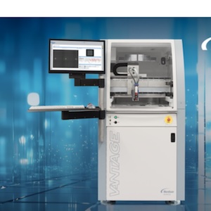
PTI, one of the world’s top OSAT (Outsourced Semiconductor Assembly and Test) companies, worked with the Nordson applications team to set up a comprehensive PLP demonstration that achieved high-quality, void-free underfill results at scale, using the industry-leading ASYMTEK Vantage® Series fluid dispensing system, equipped with the ASYMTEK IntelliJet® Jetting system. Nordson’s precision technology mitigated warpage and optimized fluid flow while decreasing cycle time by almost 30%.
PLP offers a path to managing the complexity of larger die sizes and higher-density designs while maintaining manufacturability and cost efficiency as the semiconductor industry transitions from 300-mm wafers to panels. PTI is enabling PLP applications that are designed to meet the semiconductor industry’s growing demands to serve AI, high-performance computing (HPC), and chiplet-based architectures.
Underfill has been pivotal in semiconductor packaging since the adoption of flip-chips in the 1990s. As applications have become more demanding, particularly in high-performance CPUs, GPUs, and advanced architectures like flip-chip and 2.5D/3D ICs, the importance of underfilling to enhance mechanical reliability and thermal performance has grown. Since the beginning, Nordson developed innovations for underfill processes as the industry evolved from PC board, substrate, wafer, and now panel applications.
Nordson’s distributor, Jetinn Global Equipment Ltd., supported the advancements discussed in this case study by investing in demonstration equipment and providing expert technical support.
Share on:


Testimonial
"We’re proud to call I-Connect007 a trusted partner. Their innovative approach and industry insight made our podcast collaboration a success by connecting us with the right audience and delivering real results."
Julia McCaffrey - NCAB GroupSuggested Items
Secure Semiconductor Manufacturing Acquires Full SMT Line from Manncorp
09/11/2025 | ManncorpSecure Semiconductor Manufacturing, LLC (SSM), an American-owned company dedicated to producing secure printed wiring boards and advanced assembly solutions in the MidWest USA, today announced the acquisition of a complete surface mount technology (SMT) line from Manncorp.
MEMS & Imaging Sensors Summit to Spotlight Sensing Revolution for Europe’s Leadership
09/11/2025 | SEMIIndustry experts will gather November 19-20 at the SEMI MEMS & Imaging Sensors Summit 2025 to explore the latest breakthroughs in AI-driven MEMS and imaging optimization, AR/VR technologies, and advanced sensor solutions for critical defence applications.
Direct Imaging System Market Size to Hit $4.30B by 2032, Driven by Increasing Demand for High-Precision PCB Manufacturing
09/11/2025 | Globe NewswireAccording to the SNS Insider, “The Direct Imaging System Market size was valued at $2.21 Billion in 2024 and is projected to reach $4.30 Billion by 2032, growing at a CAGR of 8.68% during 2025-2032.”
Tokyo Electron Establishes New Development Site in Bengaluru, India
09/10/2025 | TELTokyo Electron announced the establishment of a new development site in Bengaluru, Karnataka, India.
SEMI Showcases New Conductor™ Intelligence Platform for Enhanced Global Supply Chain Collaboration
09/10/2025 | SEMISEMI, the industry association serving the global semiconductor and electronics design and manufacturing supply chain, announced its new ConductorTM intelligence platform for enhanced supply chain management at SEMICON Taiwan.