


 Happy’s Tech Talk #43: Engineering Statistics Training With Free Software
 It’s Only Common Sense: Stop Whining About the Market—Outwork It
 Dan’s Biz Bookshelf: 'A View from the Top: Moving from Success to Significance'


Koh Young Showcases Advanced Dimensional Metrology and Inspection Solutions for Semiconductor and Wafer-Level Packaging at SEMICON India
August 14, 2025 | Koh YoungEstimated reading time: 1 minute
Koh Young, the industry leader in True 3D™ measurement-based dimensional metrology and inspection solutions, will present its latest advancements for semiconductor and advanced packaging applications in Hall 1 Booth 1086 during SEMICON India 2025 held September 2-4, 2025, at Yashobhoomi (IICC), New Delhi, India.
With nearly 25,000 systems installed at over 3,800 manufacturing sites, Koh Young set the standard in automated optical inspection for the electronics manufacturing industry. Building on that foundation, it expanded into semiconductor manufacturing with higher‑resolution optics, advanced measurement algorithms, and solutions engineered for metrology and inspection of wafer‑level packages (WLP), system‑in‑package (SiP), and ultra high-density interconnect applications.
As an exhibitor, Koh Young will highlight how its AI‑powered metrology and inspection solutions can help manufacturers meet the exacting demands of advanced packaging and semiconductor processes. From wafer‑level to SiP, Koh Young technology delivers accurate, repeatable data to enable smarter process control, higher yields, and supports zero‑defect production goals.
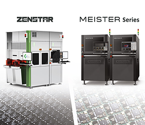
Dimensional Metrology for Advanced Packaging
Koh Young’s Meister Series is purpose‑built for advanced packaging, including SiP, WLP, and die stacking metrology. These systems provide ultra‑high‑resolution 2D/3D measurement to manage features and tolerances in next‑generation designs. Complementing the Meister Series, the ZenStar delivers wafer‑level dimensional metrology to detect and quantify critical parameters at the earliest stage, ensuring only known‑good components advance. Together, these platforms help manufacturers maintain process windows, improve yield, and reduce costly rework.
As India accelerates its Make in India semiconductor mission, Koh Young is committed to supporting local and multinational manufacturers in building a competitive, self‑reliant ecosystem for advanced electronics. By delivering robust, data‑driven metrology and inspection, Koh Young enables domestic production that meets the stringent standards of global supply chains.
“India’s semiconductor industry is entering an unprecedented growth phase,” said Peter Shin, General Manager, Koh Young South‑East Asia. “Our advanced dimensional metrology and inspection solutions empower manufacturers to deliver world‑class quality, improve productivity, and strengthen India’s position in the global semiconductor market.”
Share on:


Testimonial
"Our marketing partnership with I-Connect007 is already delivering. Just a day after our press release went live, we received a direct inquiry about our updated products!"
Rachael Temple - AlltematedSuggested Items
Now Available—The Companion Guide to… SMT Inspection: Today, Tomorrow, and Beyond: Mastering Metrology for Advanced Semiconductor Packages
10/03/2025 | I-Connect007I-Connect007 is pleased to announce the release of an 18-page resource for engineers, technologists, and decision-makers in electronics manufacturing: The Companion Guide to SMT Inspection: Today, Tomorrow, and Beyond: Mastering Metrology for Advanced Semiconductor Packages.
Koh Young to Showcase Semiconductor Metrology and Advanced Packaging Inspection Solutions at iMAPS 2025 in San Diego
09/25/2025 | Koh Young TechnologyKoh Young Technology, the global leader in True 3D measurement-based metrology and inspection solutions, will make its first appearance at iMAPS 2025, the premier event for microelectronics and advanced packaging, taking place September 29 through October 2, 2025 in San Diego.
EV Group Achieves Breakthrough in Hybrid Bonding Overlay Control for Chiplet Integration
09/12/2025 | EV GroupEV Group (EVG), a leading provider of innovative process solutions and expertise serving leading-edge and future semiconductor designs and chip integration schemes, today unveiled the EVG®40 D2W—the first dedicated die-to-wafer overlay metrology platform to deliver 100 percent die overlay measurement on 300-mm wafers at high precision and speeds needed for production environments. With up to 15X higher throughput than EVG’s industry benchmark EVG®40 NT2 system designed for hybrid wafer bonding metrology, the new EVG40 D2W enables chipmakers to verify die placement accuracy and take rapid corrective action, improving process control and yield in high-volume manufacturing (HVM).
Koh Young Highlighting Dimensional Metrology & Inspection Solutions at the Binghamton University Electronics Packaging Symposium
08/12/2025 | Koh YoungKoh Young, the industry leader in True 3D™ measurement-based dimensional metrology and inspection solutions, is proud to announce its sponsorship and participation in the 36th Annual Electronics Packaging Symposium (EPS), hosted at the GE Aerospace Research Campus in Niskayuna, New York, on September 03-04, 2025.
TRI's Advanced WLP and Back-End Solutions at SEMICON Taiwan 2025
08/11/2025 | TRITest Research, Inc. (TRI), the leading test and inspection systems provider for the electronics manufacturing industry, will join SEMICON Taiwan held at Taipei Nangang Exhibition Center, Hall 1 – 1F from September 10 - 12, 2025.