


 Defense Speak Interpreted: The Autonomous Plane Battle—Skyborg Vs. Loyal Wingman
 American Made Advocacy: Congress Back from Break With Work To Do
 Beyond the Board: What Companies Need to Know Before Entering the MilAero PCB Market


STMicroelectronics to Advance Next-generation Chip Manufacturing Technology with New PLP Pilot Line in Tours, France
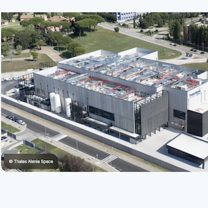
September 17, 2025 | STMicroelectronicsEstimated reading time: 3 minutes
STMicroelectronics, a global semiconductor leader serving customers across the spectrum of electronics applications, today announced new details regarding the development of the next generations of Panel-Level Packaging (PLP) technology through a pilot line in its Tours site, France, which is expected to be operational in Q3 2026.
PLP is an advanced, automated chip packaging and test process technology bringing increased manufacturing efficiency and reducing costs, and a key enabler for creating the next generation of smaller, more powerful, and cost-effective electronic devices. The large-area carrier in PLP (large rectangular shapes in place of circular wafers) enables higher manufacturing throughput, making it a more efficient solution for high-volume production. Building on its first-generation PLP line in operation in Malaysia and its global technology R&D network, ST plans to develop the next generations of its PLP technology to maintain its technological leadership and extend the use of PLP across many other ST products for automotive, industrial and consumer applications.
“The development of our PLP capabilities in our Tours site is aimed at advancing this innovative approach to chip packaging and test manufacturing technology, boosting efficiency and flexibility so it can be rolled out across a wide portfolio of applications, including RF, analog, power and microcontrollers. A multidisciplinary team of experts in manufacturing automation, process engineering, data science and analytics, as well as technology and product R&D, will collaborate on this program, which is a key part of a larger strategic initiative focused on heterogeneous integration – a scalable, efficient new approach to chip integration,” said Fabio Gualandris, President Quality, Manufacturing and Technology of STMicroelectronics. “With our fab in Malta, ST has already demonstrated its capability to deliver high-performing chip packaging and test in Europe. As we reshape our global manufacturing footprint, this new initiative in Tours will expand our process, design and manufacturing innovation capabilities supporting the development of next-generation chips in Europe”.
The development of the new PLP pilot line in Tours is supported by a capital investment of over $60 million, already allocated as part of the company-wide program to reshape the Company’s manufacturing footprint. Additional synergies are expected with the local R&D ecosystem, including the CERTEM R&D center. As previously announced, this program is focused on advanced manufacturing infrastructure and brings redefined missions for some sites in France and Italy to support their long-term success.
Technical note on PLP
For decades, the industry has relied on wafer-level packaging (WLP) and flip-chip technology to connect silicon chips to external circuitry. However, as devices become smaller and more complex, these methods have begun to reach their limits in terms of scalability and cost-effectiveness. For advanced packaging, different approaches exist or are under development; PLP is one of them.
Panel Level Packaging is a method where multiple ICs are packaged on a single, larger rectangular substrate panel, rather than on individual circular wafers. This allows for more ICs to be processed simultaneously, reducing costs and improving throughput.
ST has not only adopted PLP-DCI but has also been at the forefront of its development since 2020. The company’s research and development teams have worked to prototype and scale the technology, culminating in a state-of-the-art PLP-DCI process currently in production at very high volumes of over 5 million units per day on a highly automated line using very large, 700x700mm panels.
ST’s PLP technology focuses on Direct Copper Interconnect (DCI). Direct copper interconnections replace the traditional wire connections of chips with their encapsulation support. DCI is the process by which these ICs are electrically connected to the panel substrate using copper, which is known for its excellent electrical conductivity. DCI offers superior performance compared to traditional methods that use solder bumps, which can be less reliable. This technology with direct connection without wire supports new product development by reducing power losses (such as resistance and inductance), enhancing heat dissipation and enabling miniaturization. This leads to better overall power density.
PLP-DCI also allows the integration of multiple chips within advanced packages, known as System in Package (SiP).
Share on:


Testimonial
"Advertising in PCB007 Magazine has been a great way to showcase our bare board testers to the right audience. The I-Connect007 team makes the process smooth and professional. We’re proud to be featured in such a trusted publication."
Klaus Koziol - atgSuggested Items
Advanced Rework Technology Inspires Students at National Manufacturing Day 2025
10/08/2025 | A.R.T. Ltd.Advanced Rework Technology Ltd. (A.R.T.), a leading independent IPC-accredited training provider, joined forces with Jaltek, a UK-based electronics manufacturer with over 35 years’ experience in designing and producing high-quality electronic products, to deliver hands-on workshops for students during National Manufacturing Day 2025.
ZenaTech Advances Taiwan Facility to Commissioning for NDAA-Compliant Drone Component Production
10/08/2025 | Globe NewswireZenaTech, Inc., a business technology solution provider specializing in AI (Artificial Intelligence) drones, Drone as a Service (DaaS), Enterprise SaaS, and Quantum Computing solutions, announces that its Taipei, Taiwan-based Spider Vision Sensors (SVS) subsidiary has advanced to the commissioning phase and assembly line setup at its recently leased 16,000 square-foot drone components manufacturing facility.
Amkor Technology Breaks Ground on New Semiconductor Advanced Packaging and Test Campus in Arizona
10/08/2025 | Amkor TechnologyAmkor Technology, Inc., a leading provider of semiconductor packaging and test services, in collaboration with the Trump Administration, announces the groundbreaking and expanded planned investment of its new state-of-the-art outsourced semiconductor advanced packaging and test campus in Arizona.
The Training Connection, LLC Welcomes Industry Veteran Jack Harris to Lead Training Partnerships
10/07/2025 | The Training Connection LLCThe Training Connection, LLC (TTC-LLC), a premier provider of test engineering and development training, is proud to announce that Jack Harris, one of the most recognized names in electronics manufacturing training and technical development, has joined the company as Relationship Lead, Training.
RECIF Technologies Adopts Agileo Automation’s Combined Speech Scenario and E84 PIO Box Solution
10/07/2025 | Agileo AutomationAgileo Automation, a leading provider of control and connectivity solutions for global semiconductor manufacturing equipment, announced at Booth #877 at SEMICON West 2025 that RECIF Technologies has adopted its combined Speech Scenario and E84 PIO Box solution to test its wafer handling and tracking equipment for E84 and SECS/GEM compliance.