


 Trouble in Your Tank: At 40 GHz, Everything Matters, Part 2
 It’s Only Common Sense: Stop Watching the Headlines and Start Watching the Opportunity
 The Right Approach: The Pros and Cons of PCB Vertical Integration


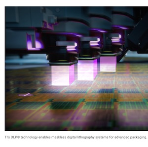
Texas Instruments is enhancing the next generation of digital lithography with the introduction of the DLP991UUV digital micromirror device (DMD), the company’s highest resolution direct imaging solution to date. With 8.9 million pixels, sub-micron resolution capabilities and a data rate of 110 gigapixels per second, the device eliminates the need for expensive mask technology while delivering the scalability, cost-effectiveness and precision needed for increasingly complex packaging.
Why it matters
Maskless digital lithography machines - which project light for etching circuit designs on materials without a photomask or high-end stencil - are becoming increasingly popular for the manufacturing of advanced packaging. Advanced packaging combines multiple chips and technologies into a single package, enabling high-computing applications, such as data centers and 5G, to have systems that are smaller, faster, and more power-efficient.
With TI DLP technology, system assembly equipment manufacturers can leverage maskless digital lithography to achieve the high-resolution printing at scale necessary for advanced packaging. The new DLP991UUV acts as a programmable photomask, offering precise pixel control with reliable high-speed performance.
“Just as we redefined cinema by enabling the transition from film to digital projection, TI’s DLP technology is once again at the forefront of a major industry shift,” said Jeff Marsh, vice president and general manager of DLP technology at TI. “We're enabling the creation of maskless digital lithography systems that empower engineers around the world to breakthrough the current limits of advanced packaging and bring powerful computing solutions to market.”
For more information, read the company blog, “Beyond the mask: How DLP® technology is enabling new computing solutions with advanced packaging.”
More details
Improving advanced packaging requires lithography technology to be more cost-effective, scalable and precise. By eliminating mask infrastructure and its associated expenses, TI's DLP technology helps significantly reduce manufacturing costs while providing the flexibility to make real-time design adjustments without physical mask changes. The technology can achieve sub-micron precision on a substrate of any size, which directly translates to higher throughput, improved yield and fewer defects. These are significant advantages as advanced packaging manufacturers seek to meet escalating demands for high-bandwidth, low-power components in AI systems and 5G networks.
The DLP991UUV is the latest and leading device of TI's direct imaging portfolio. Key features of the device include:
- Highest resolution in the portfolio, offering more than 8.9 Megapixels
- Fastest processing speed of up to 110 Gigapixels per second
- Power levels of 22.5W/cm² at 405nm
- Ability to operate at wavelengths as low as 343nm
- Smallest mirror pitch in the portfolio of 5.4um
Texas Instruments DLP® technology harnesses the power of millions of microscopic mirrors to deliver leading high-resolution display and advanced light control solutions. The technology enables applications ranging from the projection of brilliant 4K content in home theaters to enhanced road safety with intelligent automotive lighting and high-precision lithography and machine vision systems for next-generation industrial manufacturing.


