


 Trouble in Your Tank: At 40 GHz, Everything Matters, Part 2
 It’s Only Common Sense: Stop Watching the Headlines and Start Watching the Opportunity
 The Right Approach: The Pros and Cons of PCB Vertical Integration


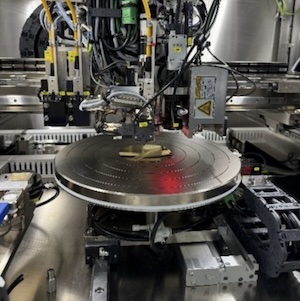
Following further investment in advanced packaging capability at its BP2 OSAT facility, CIL has brought on-line the UK’s first PacTech SB² – Jet solder ball laser reflow system. The SB² – Jet system is a three laser fully automatic balling system capable of attaching ball sizes ranging from 60um to 760um and up to 300mm wafer sizes. This will enable CIL to provide OSAT services for wafer, interposer, Flip Chip, WLCSP, CSP, PCB bumping through to BGA balling and re-balling.
As well as ball sizes from 60um to 760um, CIL will be offering advanced packaging ball attach using a selection of varying solder alloys for different market applications, these include
SAC305 - Standard RoHS alloy for most applications
SAC405 - Standard RoHS alloy for some applications
SACQ - Offers superior fatigue resistance and improved board-level reliability over SAC405 or SAC305
Tin / Lead - Defence, Mil Aero, Aerospace & Space requirement
Bismuth - Medical & Biomedical devices
CIL’s WLCSP / Flip Chip packaging services will be engaged in wide-range of industry applications, including defence, aerospace, automotive, premium motorsport, commercial, communication, industrial power, 5G and RF and many more. They are suitable for numerous assembly and packaging applications, such as:
- Flip Chip Package on Package (FC PoP)
- 3D Integrated Circuit (IC)
- 5D Interposer
- Flip Chip
- Embedded Integrated Circuit (IC)
- Fan-Out Wafer Level Packaging (FO WLP)
- Wafer Level Chip Scale Packaging (WLCSP)
- Chip Scale Packaging (CSP)
- Ball Grid Array (BGA)
- Ball Grid Array re-balling
- Printed Circuit Board (PCB) balling
The main process CIL is enabling in the UK is the manufacture of Flip Chip and WLCSP devices. These two devices are sometime confused, and they are defined as such
- Flip Chip - refers to bumps on semiconductor wafers which are in the range of 50 to 200 µm in height and are usually assembled using and underfill material between the die and the substrate
- WLCSP - refers to bumps that are in the range of 200 to 500 µm in height and are usually assembled without an underfill material
The SB² – Jet is the flagship platform of PacTech’s leading edge solder jetting technology with the high precision gantry is the most advanced system for automated high-speed sequential solder ball attach and laser reflow. With accurate, precise and reliable performance proven in mass volume production environment, the large working area of this model is highly flexible for a variety of different microelectronic substrates and applications. CIL’s comprehensive version of the SB² – Jet is complete with a vision and pattern-recognition system, an after-bump 2D inspection and an additional repair unit, wafer handling solution customizable to support customer-specific products and carriers such as conveyor, robot or reel-to-reel system, this machine is ready for in-line production integration.


