


 Happy’s Tech Talk #29: Bend-to-Install Semi-flex FR-4


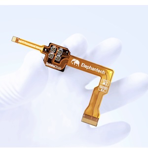
Elvia PCB: The Future of PCB Manufacturing, Technologies
August 17, 2012 | Richard Ayes, I-Connect007Estimated reading time: 8 minutes
Editor's Note: This article originally appeared in the July 2012 issue of The PCB Magazine.
Since its acquisition of French-based CIRE Group in September 2011, PCB maker Elvia PCB Group has become one of the major PCB groups in Europe, with total sales reaching 77 million Euro in 2011. The acquisition enabled Elvia PCB to expand its market coverage to aerospace and defense, IT, rail, automotive electronics, power, and lighting, to name a few, as well as hold certifications such as NADCAP and ISO-TS-16949.
Elvia PCB is now organized into four clusters: space-defense-aerospace-rail, IT and industrial, power and lighting, and automotive. This organization enables each plant to focus on specific technologies. The company claims to have the advantage of having reached a critical mass, while retaining the agility inherent in its manufacturing organization. Elvia PCB has a total of nine facilities, with production adapted to the markets it is catering to. Elvia PCB also offers a wide range of products, including HDIs, multilayer, flex, rigid-flex, sculptured flex, metal-backed/IMS, and microwave PCBs.
 In this interview with I-Connect007, CEO Bruno Cassin reflects on the company's business prospects this year, the latest technology developments in the company, and the issues PCB makers are facing, including more complex products and highly reliable PCBs. Excerpts:
I-Connect007: As electronics find their way into more applications, for example, automotive electronics or aerospace/defense, the board requirements also tend to get more complex: that is, they require higher reliability, smaller real estate, even more layers, and finer lines and pitches. How does your company adapt to such changes, and what process improvements have been implemented to address such issues?
Bruno Cassin: Elvia PCB has a strong competitive advantage in this respect as every plant is dedicated to specific technology. For example, our Normandy facility is focused on HDI multilayers. In Brittany, our plant is dedicated to flex and rigid-flex and is a leading manufacturer in the microwave PCB market. Our facility known as “BREE,” located south of Paris, is dedicated to metal-backed/IMS and thick copper. These are just a few examples.
Regarding reliability, we apply the experience gained from various fields such as aerospace and automotive to other applications. We have two laboratories to qualify our new technologies, so even in new developments, we guarantee high-reliability products at even the earliest phases of manufacturing.
I-Connect007: During the past two to three years, what were the biggest changes that you have observed in the PCB manufacturing industry in terms of: (a) materials; (b) manufacturing processes; and (c) final board products?
Bruno Cassin: For materials, clearly both the user requirements and the materials available have largely diversified, and we are now very much using specific materials, each of them dedicated to specific applications. In processes, there are two major trends: density and power. Density remains a key driver, with more and more small holes requiring both mechanical and laser drilling. This is where we are concentrating our investments currently.
The PCB is becoming more and more a solution to combine power and data processing, driven by requirements in automotive electronics, renewable energy, and lighting. We have a facility with dedicated processes, so we are able to process very thick copper. We are currently developing substantial know-how with new projects. Meanwhile, both laser and LED imaging are now increasingly being adopted.
I-Connect007: When it comes to fabrication costs, surely they are higher today compared to five or 10 years ago. What strategies has Elvia PCB adopted or been implementing to address the cost of PCB production?
Bruno Cassin: I am not convinced that fabrication costs are higher today compared to 10 years ago. Here are a few reasons to explain why we are still very aggressive in our cost model: Elvia PCB has reached a critical mass which enables it to optimize its sourcing and negotiate material prices. In regard to productivity, by specializing our plants, and by developing automation when possible, we have been able to improve our productivity and plan to continue to do so going forward. So, we do not consider costs to be increasing.
However, we are also facing key issues such as the increase of the price of gold, but we can propose alternatives to avoid those cost increases. On the other hand, we can never guarantee base material price stability.
I-Connect007: What can you say about the future of the PCB manufacturing industry? What do you think are the key changes that would impact and effect changes in production processes, and materials and equipment used?
Bruno Cassin: Globally, the PCB industry will continue to grow, but the requirements are changing considerably; electronics is more and more widespread, and technical requirements are more and more diversified, so the PCB manufacturer has to adapt to this diversity.
The PCB manufacturer can adapt in two ways, particularly regarding the European market. Firstly, we can adapt through innovation, co-design and pro-activeness. Today, one can buy a standard, double-sided or multilayer board anywhere, but the future is not really going to be focused on those technologies. Secondly, each of the new developments require more specificity, such as microwaves utilizing specific materials. PCB technology must increasingly be considered not only in terms of the PCB, but increasingly to integrate functions that replace systems. European PCB manufacturers need to be able to offer experience, innovation, manufacturing capability and cost-efficient solutions, which is what we are doing within the Elvia PCB Group.
I-Connect007: Do you think the industry is ready to adapt to such changes?
Bruno Cassin: Yes and no. Yes, as advanced know-how has been developed over time, our business has always been linked to evolutions. At Elvia PCB, our manufacturing model is quite unique; we propose a genuine one-stop shop organization so that we can react to any technical demand. We are also able to support our customers from the co-design and prototype stages, as well as for production runs.
Yes, if we continue to concentrate more effort on innovation, not only for equipment but also for people. More engineers are required to speed up those new developments, to be the expert on the manufacturing side.
However, we also know our limits. Large volumes of standard PCBs are no longer destined for production in Europe, so our growth requires much more effort. In simple terms, we have to be sure that our R&D efforts will pay a return for us sooner or later. This is also something we must discuss with our customers. It is in the interest of our customers to maintain strong PCB manufacturers in Europe, so we must develop more win-win partnerships with them.
I-Connect007: Are you seeing any other new technologies that might complement or be an alternative to traditional printed circuit connections? What about optical interconnects?
Bruno Cassin: Yes, definitely. I am personally not so sure about optical interconnects, as this has been talked about for 20 years already. Maybe this will become a real requirement, but there are many other new technologies arising, such as thermal management, thick copper technologies, 3D PCBs using various technologies, very dense and very small PCBs, microwave boards with a very specific build-up, and new finishes to bypass the crazy price increases of other finishes, to name a few.
I-Connect007: What can you say about the overall PCB growth this year and the next? From a geographical standpoint, in which regions worldwide do you see greater demand growth?
Bruno Cassin: Since 2000, we have seen a drastic slowdown in Europe and the United States, while Asia has almost double-digit growth. In my opinion, this trend cannot be stopped, but we can see a few serious reasons for not continuing down this path: the requirements are diversifying, and close proximity between PCB design and project development is essential. In various fields like the automotive, defense and medical electronics, there are increasing issues with intellectual property. I believe that in the future, not every project will be sent to the other side of the world purely to make some cost savings.
Our customers are starting to realize that they need to keep some know-how if they want to survive in the future. In many cases, the PCB is a critical and strategic brick in their systems, so they need us. Global requirements will continue to increase, but the share which stays in Europe will definitively increase. Our target is to be there when our customers need us.
I-Connect007: How is business shaping up so far this year?
Bruno Cassin: We saw a significant slowdown in the IT/industrial cluster in the second half of 2011, with no recovery so far. In the meantime, the aerospace/defense business is quite strong. In the automotive and power and lighting clusters, we have a significant number of projects at the development stage. This shows a potential for significant growth by end-2012/early 2013.
I-Connect007: Which industry sectors would you say are the major drivers for your growth?
Bruno Cassin: Currently, the aerospace/defense cluster is growing, but we believe that growth from the automotive and power and lighting clusters will overtake this within one year.
I-Connect007: Please enlighten us on some of the latest initiatives or business plans for the company this year.
Bruno Cassin: As we explained before, Elvia PCB Group is a major player in Europe, with business activities in all sectors, so I will just mention a few examples:
- Microwave PCBs are one of our leading product ranges. For defense requirements, we developed micro-BGA PCBs combined with antennas. We believe those technologies will also have a future in civilian products.
- Very thick backplanes for the aerospace industry.
- Very thick copper; the bus bars we developed for the automotive industry have now also been adapted for the renewable energy and aerospace sectors.
- A project for an automotive customer, wherein we are combining HDI and microwave PCBs using specific materials, as well as with low cost targets.
In all of our facilities, our engineers are verflxy active with new developments, which, we are convinced, are our future. Customers are also increasingly convinced that their future is very closely linked to our future, so we are learning a new way of doing business—by developing strong partnerships. And this really works.
 Bruno Cassin, chairman and CEO of Elvia PCB Group, started his carrier with Schlumberger, before joining Alcatel in 1984. In 1992, Bruno was appointed CEO of Alcatel Coutances (Normandy, France), and in 2003, he led an MBO of this high-tech facility specialized in the manufacture of HDI Multilayer PCBs.
Share on:


