


 Global PCB Connections: Rigid-flex and Flexible PCBs—The Backbone of Modern Electronics
 Flexible Thinking: The Key to a Successful Flex Circuit Design Transfer
 Happy’s Tech Talk #29: Bend-to-Install Semi-flex FR-4


Inkjet-printed Liquid Metal Could Bring Wearable Tech, Soft Robotics
April 8, 2015 | Purdue UniversityEstimated reading time: 2 minutes
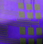
New research shows how inkjet-printing technology can be used to mass-produce electronic circuits made of liquid-metal alloys for "soft robots" and flexible electronics.
Elastic technologies could make possible a new class of pliable robots and stretchable garments that people might wear to interact with computers or for therapeutic purposes. However, new manufacturing techniques must be developed before soft machines become commercially feasible, said Rebecca Kramer, an assistant professor of mechanical engineering at Purdue University.
"We want to create stretchable electronics that might be compatible with soft machines, such as robots that need to squeeze through small spaces, or wearable technologies that aren't restrictive of motion," she said. "Conductors made from liquid metal can stretch and deform without breaking."
A new potential manufacturing approach focuses on harnessing inkjet printing to create devices made of liquid alloys.
"This process now allows us to print flexible and stretchable conductors onto anything, including elastic materials and fabrics," Kramer said.
A research paper about the method will appear on April 18 in the journal Advanced Materials. The paper generally introduces the method, called mechanically sintered gallium-indium nanoparticles, and describes research leading up to the project. It was authored by postdoctoral researcher John William Boley, graduate student Edward L. White and Kramer.
A printable ink is made by dispersing the liquid metal in a non-metallic solvent using ultrasound, which breaks up the bulk liquid metal into nanoparticles. This nanoparticle-filled ink is compatible with inkjet printing.
"Liquid metal in its native form is not inkjet-able," Kramer said. "So what we do is create liquid metal nanoparticles that are small enough to pass through an inkjet nozzle. Sonicating liquid metal in a carrier solvent, such as ethanol, both creates the nanoparticles and disperses them in the solvent. Then we can print the ink onto any substrate. The ethanol evaporates away so we are just left with liquid metal nanoparticles on a surface."
After printing, the nanoparticles must be rejoined by applying light pressure, which renders the material conductive. This step is necessary because the liquid-metal nanoparticles are initially coated with oxidized gallium, which acts as a skin that prevents electrical conductivity.
"But it's a fragile skin, so when you apply pressure it breaks the skin and everything coalesces into one uniform film," Kramer said. "We can do this either by stamping or by dragging something across the surface, such as the sharp edge of a silicon tip."
The approach makes it possible to select which portions to activate depending on particular designs, suggesting that a blank film might be manufactured for a multitude of potential applications.
"We selectively activate what electronics we want to turn on by applying pressure to just those areas," said Kramer, who this year was awarded an Early Career Development award from the National Science Foundation, which supports research to determine how to best develop the liquid-metal ink.
The process could make it possible to rapidly mass-produce large quantities of the film.
Future research will explore how the interaction between the ink and the surface being printed on might be conducive to the production of specific types of devices.
"For example, how do the nanoparticles orient themselves on hydrophobic versus hydrophilic surfaces? How can we formulate the ink and exploit its interaction with a surface to enable self-assembly of the particles?” she said.
The researchers also will study and model how individual particles rupture when pressure is applied, providing information that could allow the manufacture of ultrathin traces and new types of sensors.
Share on:


Testimonial
"The I-Connect007 team is outstanding—kind, responsive, and a true marketing partner. Their design team created fresh, eye-catching ads, and their editorial support polished our content to let our brand shine. Thank you all! "
Sweeney Ng - CEE PCBSuggested Items
ASE, Analog Devices Announce Strategic Collaboration
10/21/2025 | BUSINESS WIREASE Technology Holding Co., Ltd., and Analog Devices, Inc., announced strategic joint efforts in Penang, Malaysia with the signing of a binding Memorandum of Understanding.
Flex Sites in Brazil and Mexico Recognized as Manufacturing Leaders by the Association for Manufacturing Excellence
10/21/2025 | PRNewswireFlex announced that its sites in Manaus, Brazil, and our plastics operations in Guadalajara, Mexico, each received an Excellence Award from the Association for Manufacturing Excellence (AME), demonstrating global leadership in continuous improvement and operational excellence.
Global Electronics Association Releases Fall Schedule of Instructor-led Courses
10/20/2025 | Corey Lynn, Global Electronics AssociationWhether you’re looking to enhance your PCB design skills, explore advanced packaging technologies, or deepen your understanding of reliability, these Global Electronics Association courses deliver high-impact learning from the best in the industry. Here are a few starting this week.
Fabrinet Announces Retirement of Founder and Chairman Tom Mitchell After 25 Years of Visionary Leadership
10/20/2025 | FabrinetFabrinet, a leading provider of advanced optical packaging and precision optical, electro-mechanical and electronic manufacturing services to original equipment manufacturers of complex products, announced the retirement of company founder and Chairman, David T. (Tom) Mitchell, after 25 years of visionary leadership.
Marcy’s Musings: The Legislative Outlook—Helping or Hurting?
10/20/2025 | Marcy LaRont -- Column: Marcy's MusingsJust before we were ready to publish our October issue of PCB007 Magazine, some breaking news from the White House, unfortunately (but perfectly) parlayed into why the topic of this month’s issue has been so important to cover in great depth.