


 Flexible Thinking: Designing Flex Circuits for Dynamic Reliability
 Global PCB Connections: Rigid-flex and Flexible PCBs—The Backbone of Modern Electronics
 Happy’s Tech Talk #29: Bend-to-Install Semi-flex FR-4


ESI Supplies Model 5335 Laser Processing System to PFC
June 9, 2015 | Business WireEstimated reading time: 2 minutes
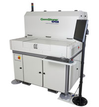
Electro Scientific Industries, Inc., an innovator in laser-based manufacturing solutions for the micro-machining industry, today announced that PFC Flexible Circuits Limited has selected the Model 5335 Laser Processing System to expand its high density interconnect (HDI) flexible circuit manufacturing capabilities. Based in Scarborough, Ont., Canada, PFC is a North American leader in flexible circuit design, manufacture and assembly.
“PFC has been supplying fine line technology for the past eight years. Now, with the addition of the Model 5335, we can support true HDI flex technologies,” said Steve Kelly, President of PFC Flexible Circuits. “This laser processing system from ESI will allow us to make smaller vias, blind and buried vias, and to cut smaller features in HDI circuits. We’re seeing strong market interest in HDI across multiple industries ranging from consumer and medical devices to military and aerospace.”
PFC chose the ESI Model 5335 in part because of its high throughput capabilities compared to alternatives. For example, the ESI Model 5335 can drill 50 micron blind vias at a rate of 32,000 holes per minute. This performance is made possible by Third Dynamics™, a patented high-speed beam positioning technology that enables fast and accurate routing and drilling of flexible circuits.
“We were looking to update our drilling technology without losing throughput,” said Anish Somaiya, Vice President, PFC Flexible Circuits. “The Model 5335 not only will significantly increase our drilling throughput and give us a technological edge over many of our competitors but also will save floor space in our drilling area.”
The ESI Model 53XX family is widely regarded as the industry standard for laser processing across the flexible circuit and interconnect industry. Over 1,200 ESI laser processing systems are installed worldwide and are in use at nine of the top 10 flex circuit manufacturers. These systems offer industry-leading drill, routing, patterning, and skiving performance.
“We are extremely pleased that PFC has decided to incorporate ESI laser processing technology into its HDI and flexible circuit manufacturing processes,” said Ed Grady, CEO of ESI. “We look forward to being a part of PFC’s long-term success and helping them meet their most challenging customer demands.”
About PFC
PFC Flexible Circuits designs, manufactures and assembles flexible printed circuits, all under one roof. Circuit types include single- and double-sided, multi-layer and rigid flex. PFC can provide 50 micron line and space in production and assemble circuits using 1005 components. Specialties include high-speed low-loss, impedance-controlled circuits. PFC offers a large library of UL approved materials and is ISO 9001 and 13485 approved. For more information go to: www.pfcflex.com.
About ESI
ESI's integrated solutions allow industrial designers and process engineers to control the power of laser light to transform materials in ways that differentiate their consumer electronics, wearable devices, semiconductor circuits and high-precision components for market advantage. ESI's laser-based manufacturing solutions feature the micro-machining industry's highest precision and speed, and target the lowest total cost of ownership. ESI is headquartered in Portland, Ore., with global operations from the Pacific Northwest to the Pacific Rim. More information is available at www.esi.com.
Share on:


Testimonial
"The I-Connect007 team is outstanding—kind, responsive, and a true marketing partner. Their design team created fresh, eye-catching ads, and their editorial support polished our content to let our brand shine. Thank you all! "
Sweeney Ng - CEE PCBSuggested Items
I-Connect007 Editor’s Choice: Five Must-Reads for the Week
05/08/2026 | Marcy LaRont, I-Connect007This week, I’ve selected some outstanding interviews that you’ll want to take note of. First, is a roundtable discussion featuring three dynamic industry cybersecurity experts. Please watch this important discussion that affects us all. Following that, I spotlight the IPC-2581 Consortium, which explains why IPC-2581 is the standard to replace Gerber data for manufacturing. Next, I am including my interview with PCBAA and AAM, who collaborated to release a short documentary on U.S. PCB manufacturing.
ASE, WUS Announce Strategic Collaboration to Build Advanced AI Packaging Hub in Kaohsiung
05/08/2026 | ASE GroupAdvanced Semiconductor Engineering, Inc. (ASE) and WUS Printed Circuit Co., Ltd. (WUS) announced today a strategic collaboration for the construction of a state-of-the-art manufacturing facility in the Nanzih Technology Industrial Park, Kaohsiung.
Foxconn, ElectroMobility Poland in Strategic Partnership to Develop Electric Vehicle Ecosystem
05/08/2026 | FoxconnHon Hai Technology Group (Foxconn) plans to accelerate the development of clean mobility in the European region in strategic partnership with state-backed ElectroMobility Poland S.A. (EMP), the key driver of an ambitious initiative to raise the technological and operational capabilities of the electric vehicle ecosystem in Poland and the broader region.
Flex Plans Cloud and Power Unit Spin-Off
05/08/2026 | FlexFlex announced that its Board of Directors has unanimously approved moving forward with a plan to spin off its Power and Cloud portfolio from Flex, creating two independent, publicly traded companies, each optimally positioned to serve their customers and create value for their shareholders.
Global Electronics Association to Testify at the Office of the U.S. Trade Representative Panel on Section 301 Structural Excess Capacity
05/08/2026 | Global Electronics AssociationChris Mitchell, Vice President for Global Government Relations at the Global Electronics Association, will testify before the Office of the U.S. Trade Representative (USTR) Panel on Section 301 Structural Excess Capacity on Friday, May 8.