


 It’s Only Common Sense Mastering the Follow-Up—The Key to Closing More Deals
 Driving Innovation: Registration in PCB Production Throughout the Process
 Dan's Biz Bookshelf: 'Getting Naked: A Business Fable'


3D Printing With Metals
June 11, 2015 | University of TwenteEstimated reading time: 2 minutes
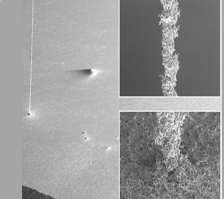
A team of researchers from the University of Twente has found a way to 3D print structures of copper and gold, by stacking microscopically small metal droplets. These droplets are made by melting a thin metal film using a pulsed laser. Their work is published on Advanced Materials.
3D printing is a rapidly advancing field, that is sometimes referred to as the 'new cornerstone of the manufacturing industry'. However, at present, 3D printing is mostly limited to plastics. If metals could be used for 3D printing as well, this would open a wide new range of possibilities. Metals conduct electricity and heat very well, and they're very robust. Therefore, 3D printing in metals would allow manufacturing of entirely new devices and components, such as small cooling elements or connections between stacked chips in smartphones.
However, metals melt at a high temperature. This makes controlled deposition of metal droplets highly challenging. Thermally robust nozzles are required to process liquid metals, but these are hardly available. For small structures in particular (from 100 nanometres to 10 micrometres) no good solutions for this problem existed yet.
Researchers from FOM and the University of Twente now made a major step towards high-resolution metal printing. They used laser light to melt copper and gold into micrometre-sized droplets and deposited these in a controlled manner. In this method, a pulsed laser is focused on a thin metal film. that locally melts and deforms into a flying drop. The researchers then carefully position this drop onto a substrate. By repeating the process, a 3D structure is made. For example, the researchers stacked thousands of drops to form micro-pillars with a height of 2 millimetres and a diameter of 5 micrometres. They also printed vertical electrodes in a cavity, as well as lines of copper. In effect, virtually any shape can be printed by smartly choosing the location of the drop impact.
High Energy
In this study, the researchers used a surprisingly high laser energy in comparison to earlier work, to increase the impact velocity of the metal droplets. When these fast droplets impact onto the substrate, they deform into a disk shape and solidify in that form. The disk shape is essential for a sturdy 3D print: it allows the researchers to firmly stack the droplets on top of each other. In previous attempts, physicists used low laser energies. This allowed them to print smaller drops, but the drops stayed spherical, which meant that a stack of solidified droplets was less stable.
In their article, the researchers explain which speed is required to achieve the desired drop shape. They had previously predicted this speed for different laser energies and materials. This means that the results can be readily translated to other metals as well.
One remaining problem is that the high laser energy also results in droplets landing on the substrate next to the desired location. At present this cannot be prevented. In future work the team will investigate this effect, to enable clean printing with metals, gels, pastas or extremely thick fluids.
Share on:


Suggested Items
Elephantech: For a Greener Tomorrow
04/16/2025 | Marcy LaRont, PCB007 MagazineNobuhiko Okamoto is the global sales and marketing manager for Elephantech Inc., a Japanese startup with a vision to make electronics more sustainable. The company is developing a metal inkjet technology that can print directly on the substrate and then give it a copper thickness by plating. In this interview, he discusses this novel technology's environmental advantages, as well as its potential benefits for the PCB manufacturing and semiconductor packaging segments.
Trouble in Your Tank: Organic Addition Agents in Electrolytic Copper Plating
04/15/2025 | Michael Carano -- Column: Trouble in Your TankThere are numerous factors at play in the science of electroplating or, as most often called, electrolytic plating. One critical element is the use of organic addition agents and their role in copper plating. The function and use of these chemical compounds will be explored in more detail.
IDTechEx Highlights Recyclable Materials for PCBs
04/10/2025 | IDTechExConventional printed circuit board (PCB) manufacturing is wasteful, harmful to the environment and energy intensive. This can be mitigated by the implementation of new recyclable materials and technologies, which have the potential to revolutionize electronics manufacturing.
Connect the Dots: Stop Killing Your Yield—The Hidden Cost of Design Oversights
04/03/2025 | Matt Stevenson -- Column: Connect the DotsI’ve been in this industry long enough to recognize red flags in PCB designs. When designers send over PCBs that look great on the computer screen but have hidden flaws, it can lead to manufacturing problems. I have seen this happen too often: manufacturing delays, yield losses, and designers asking, “Why didn’t anyone tell me sooner?” Here’s the thing: Minor design improvements can greatly impact manufacturing yield, and design oversights can lead to expensive bottlenecks. Here’s how to find the hidden flaws in a design and avoid disaster.
Real Time with... IPC APEX EXPO 2025: Tariffs and Supply Chains in U.S. Electronics Manufacturing
04/01/2025 | Real Time with...IPC APEX EXPOChris Mitchell, VP of Global Government Relations for IPC, discusses IPC's concerns about tariffs on copper and their impact on U.S. electronics manufacturing. He emphasizes the complexity of supply chains and the need for policymakers to understand their effects.