


 The Marketing Minute: Cracking the Code of Technical Marketing
 Trouble in Your Tank: Implementing Direct Metallization in Advanced Substrate Packaging


The Cool Solution to Electronics Heat Dissipation
June 11, 2015 | SLAC National Accelerator LaboratoryEstimated reading time: 3 minutes
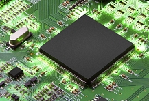
The heat that builds up in the shuttling of current in electronics is an important obstacle to packing more computing power into ever-smaller devices: Excess heat can cause them to fail or sap their efficiency.
Now, X-ray studies at the Department of Energy’s SLAC National Accelerator Laboratory have for the first time observed an exotic property that could warp the electronic structure of a material in a way that reduces heat buildup and improves performance in ever-smaller computer components.
The research was conducted, in part, at SLAC’s Stanford Synchrotron Radiation Lightsource (SSRL), a DOE Office of Science User Facility, and published this month in the print edition of Nature Materials.
Energy-bending Properties
The team studied a form of iridium oxide, Sr3Ir2O7, that belongs to a class of so-called correlated materials in which electrons can be made to behave in sync. It is a candidate for reducing the heat generated by the billions of transistors at the core of modern computers.
The researchers discovered that the material has a long-theorized property, formerly found only in 2-D materials and known as 3-D negative electronic compressibility, that is caused by its unusual electronic structure.
The electronic structure of a material is typically rigid, with distinct energy levels or “bands” that fill up as electrons are added. These levels are determined by the atomic structure and chemical composition of the material. In the study, these energy levels were observed to deform drastically, in a fluid way, as more electrons poured in, while the physical structure of the material did not change in any significant way.
“Imagine pouring water into a cup and watching the water level in the cup appear to dip as the cup deforms,” said Junfeng He, a Boston College researcher who led the study. “That’s how 3-D negative electronic compressibility appears to operate.” But in this case, it is the material’s electronic structure – which defines how it can store or flow electric current – rather than its physical structure that substantially warps as electrons are added.
Guided by theoretical calculations led by Arun Bansil, a professor of physics at Northeastern University, researchers found that a gap between different groupings of energy bands in the sample material actually shrank as electrons were added, reducing the material’s stored energy level – like the water level appearing to decline in the cup example.
In principle, using metal electrodes that have this property in the microscopic gates that regulate the flow of electrons in transistors could substantially enhance their efficiency and reduce heat buildup, said He, who will soon join SLAC as a postdoctoral researcher.
Building a Better Transistor
Rui-Hua He, an assistant professor of physics at Boston College who is a spokesperson for the research, said, “Replacing normal metals in transistors with materials like this that have negative electronic compressibility presents an intriguing alternative to current approaches, with a goal of continuing device miniaturization.” He added, “We are now working on the first demonstration of their potential application to transistors.”
Researchers employed an advanced X-ray technique at SSRL, set up and maintained by SLAC staff scientists Donghui Lu and Makoto Hashimoto, to precisely measure the electronic structure of the material. The negative electronic compressibility they found shows promise for reducing power requirements needed to move electric current around a semiconductor, for example, which would reduce the heat it generates and make electrical switching more efficient.
Previous studies had observed a 2-D version of negative electronic compressibility in other materials, but researchers said the 3-D form has greater potential for application in semiconductors because it is more compatible with their present-day architecture, can potentially be used at room temperature and can be adapted for different applications by adjusting its thickness.
“This work informs us of the importance to continually look for other new materials with novel physical properties for use in transistors and for other applications,” said Stephen Wilson, an assistant professor of materials at the University of California, Santa Barbara, who prepared the sample materials.
Participating researchers were from Boston College, Northeastern University, SLAC’s SSRL and Stanford Institute for Materials and Energy Sciences (SIMES), Lawrence Berkeley National Laboratory, Peking University in China, Hiroshima Synchrotron Radiation Center in Japan and the University of California, Santa Barbara. The work was supported by Boston College, the U.S. National Science Foundation, the W. M. Keck Foundation and the DOE Office of Basic Energy Sciences.
Share on:


Testimonial
"In a year when every marketing dollar mattered, I chose to keep I-Connect007 in our 2025 plan. Their commitment to high-quality, insightful content aligns with Koh Young’s values and helps readers navigate a changing industry. "
Brent Fischthal - Koh YoungSuggested Items
Curing and Verification in PCB Shadow Areas
09/17/2025 | Doug Katze, DymaxDesign engineers know a simple truth that often complicates electronics manufacturing: Light doesn’t go around corners. In densely populated PCBs, adhesives and coatings often fail to fully cure in shadowed regions created by tall ICs, connectors, relays, and tight housings.
Marcy’s Musings: Advancing the Advanced Materials Discussion
09/17/2025 | Marcy LaRont -- Column: Marcy's MusingsAs the industry’s most trusted global source of original content about the electronics supply chain, we continually ask you about your concerns, what you care about, and what you most want to learn about. Your responses are insightful and valuable. Thank you for caring enough to provide useful feedback and engage in dialogue.
September 2025 PCB007 Magazine: The Future of Advanced Materials
09/16/2025 | I-Connect007 Editorial TeamMoore’s Law is no more, and the advanced material solutions being developed to grapple with this reality are surprising, stunning, and perhaps a bit daunting. Buckle up for a dive into advanced materials and a glimpse into the next chapters of electronics manufacturing.
I-Connect007 Launches Advanced Electronics Packaging Digest
09/15/2025 | I-Connect007I-Connect007 is pleased to announce the launch of Advanced Electronics Packaging Digest (AEPD), a new monthly digital newsletter dedicated to one of the most critical and rapidly evolving areas of electronics manufacturing: advanced packaging at the interconnect level.
Panasonic Industry will Double the Production Capacity of MEGTRON Multi-layer Circuit Board Materials Over the Next Five Years
09/15/2025 | Panasonic Industry Co., Ltd.Panasonic Industry Co., Ltd., a Panasonic Group company, announced plans for a major expansion of its global production capacity for MEGTRON multi-layer circuit board materials today. The company plans to double its production over the next five years to meet growing demand in the AI server and ICT infrastructure markets.