


 The Marketing Minute: Cracking the Code of Technical Marketing
 Trouble in Your Tank: Implementing Direct Metallization in Advanced Substrate Packaging


Bright Light for Ultrafast Snapshots of Materials
June 16, 2015 | Lawrence Berkeley National LaboratoryEstimated reading time: 4 minutes
If you want to understand how novel phases emerge in correlated materials, including high-temperature superconductivity and nanoscale electronic order, you can obtain completely new viewpoints by taking ‘snapshots’ of underlying rapid electronic interactions. One way to do this is by delivering pulses of extremely short-wavelength UV light to a material and deriving information based on the energy and direction of travel of the emitted electrons. However, generating pulsed extreme-UV (XUV) light with the required properties for such applications is difficult to achieve.
Now, researchers at the U.S. Department of Energy (DOE)’s Lawrence Berkeley National Laboratory (Berkeley Lab) have developed a way of producing an efficient, high-repetition-rate XUV source for use in obtaining rapid, sharp images of electronic structure.
“Like taking a photo on a bright day as opposed to dim twilight, if you have a bright laser source, you can cut down the measurement noise and take excellent data because you have a lot of photons to work with” says Robert Kaindl, a condensed matter physicist with Berkeley Lab’s Materials Sciences Division, who led the work. “But there’s a catch: for experiments such as photoemission the light has to be distributed across as many pulses as possible, to avoid unwanted blurring of the measured spectra.”
Angle-resolved photoemission spectroscopy, or ARPES, is a key technique that makes use of the photoelectric effect for studying condensed matter materials. By analyzing the emitted electrons, it provides direct information about a material’s electronic structure in energy and momentum space. But standard detectors used for static measurements are about ten trillion times slower than the timescale on which electrons interact with each other. To access such microscopic timescales requires a different measurement technique based on extremely short pulses of light, on the order of 10 to 100 femtoseconds (1 fs is 10-15 s).
Robert Kaindl (left) and He Wang (right) with the high repetition-rate femtosecond XUV light source developed at Berkeley Lab.
Importantly, the photon energy of light also needs to overcome the work function of the material – with shorter wavelengths allowing for a more comprehensive view of electronic structure across energy and momentum. Thus, time-resolved ARPES requires overcoming two challenges: generating short-wavelength XUV light, and pulsing it at rapid intervals with a small number of photons per pulse, to minimize blurring from electron-electron interactions that occur after photoemission.
“It’s very difficult to generate XUV light in the first place. This is made possible by a process called high-harmonic generation, where you expose atoms to extremely strong laser fields with peak intensities of 100 Terawatts or more,” explains He Wang, who developed the source as a postdoctoral researcher at Berkeley Lab while working with Kaindl. “An electron can then tunnel out of the atom and return having picked up a lot of energy that, subsequently, it can lose by emitting an XUV photon. An important result of our work is that we achieve very efficient high-harmonic conversion into the XUV, despite operating at high repetition rates where the driving laser power has to be divided among many pulses.”
The scheme first converts infrared pulses from an amplified femtosecond laser into the UV, then gains back orders-of-magnitude in efficiency through subsequent high-harmonic conversion. At the high rate of 50,000 pulses/second, the correspondingly weak UV-driving pulses have to be focused tightly into the thin column of Krypton gas where high-harmonic generation occurs. However, this intermediate step yields a more than hundred-fold boost of XUV conversion efficiency, compared to driving the process directly with the infrared laser.
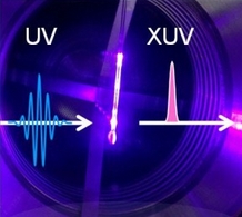
In a new technique from Berkeley Lab, UV light is used to efficiently generate XUV light at high repetition rates. Narrowband, isolated XUV harmonics around 22 eV are obtained, ideal for time-resolved ARPES studies of materials.
The Berkeley Lab study demonstrated an exceptionally bright XUV source flux, with the strongest harmonic line occurring at a wavelength of 56 nm (photon energy ~22 eV) and exceeding 1013photons/second. By accompanying these experiments with numerical calculations, Wang and Kaindl explained the observed efficiency boost through a combination of favorable electron dynamics in the intense UV laser field, together with a near-optimal coherent buildup of XUV light across the gas. In addition to flux enhancement, the setup also delivers other benefits.
“High-harmonic sources generate a series of lines with different XUV wavelengths, a show-stopper for applications like ARPES where spectra from different lines will get entangled,” says Kaindl. “In contrast, our scheme isolates a single XUV harmonic using only thin metal filters, resulting in a very compact beamline.”
The harmonic has an energy width of 72 meV, corresponding to only 0.3 % of the photon energy.
“That is extremely narrow for high harmonics, and allows us to take sharp images of the electronic structure in materials,” Wang says.
With this bright, high repetition-rate XUV source, researchers now have the opportunity to gain new insights into the physics of correlated materials by tracking their rapid, fundamental interactions across large swaths of energy and momentum space. Beyond that, these femtosecond XUV pulses represent a powerful tool for other applications such as short-wavelength metrology, coincidence and time-of-flight spectroscopy of molecules, and nanoscale imaging.
Share on:


Testimonial
"We’re proud to call I-Connect007 a trusted partner. Their innovative approach and industry insight made our podcast collaboration a success by connecting us with the right audience and delivering real results."
Julia McCaffrey - NCAB GroupSuggested Items
Curing and Verification in PCB Shadow Areas
09/17/2025 | Doug Katze, DymaxDesign engineers know a simple truth that often complicates electronics manufacturing: Light doesn’t go around corners. In densely populated PCBs, adhesives and coatings often fail to fully cure in shadowed regions created by tall ICs, connectors, relays, and tight housings.
Marcy’s Musings: Advancing the Advanced Materials Discussion
09/17/2025 | Marcy LaRont -- Column: Marcy's MusingsAs the industry’s most trusted global source of original content about the electronics supply chain, we continually ask you about your concerns, what you care about, and what you most want to learn about. Your responses are insightful and valuable. Thank you for caring enough to provide useful feedback and engage in dialogue.
September 2025 PCB007 Magazine: The Future of Advanced Materials
09/16/2025 | I-Connect007 Editorial TeamMoore’s Law is no more, and the advanced material solutions being developed to grapple with this reality are surprising, stunning, and perhaps a bit daunting. Buckle up for a dive into advanced materials and a glimpse into the next chapters of electronics manufacturing.
I-Connect007 Launches Advanced Electronics Packaging Digest
09/15/2025 | I-Connect007I-Connect007 is pleased to announce the launch of Advanced Electronics Packaging Digest (AEPD), a new monthly digital newsletter dedicated to one of the most critical and rapidly evolving areas of electronics manufacturing: advanced packaging at the interconnect level.
Panasonic Industry will Double the Production Capacity of MEGTRON Multi-layer Circuit Board Materials Over the Next Five Years
09/15/2025 | Panasonic Industry Co., Ltd.Panasonic Industry Co., Ltd., a Panasonic Group company, announced plans for a major expansion of its global production capacity for MEGTRON multi-layer circuit board materials today. The company plans to double its production over the next five years to meet growing demand in the AI server and ICT infrastructure markets.