


 Global PCB Connections: Rigid-flex and Flexible PCBs—The Backbone of Modern Electronics
 Flexible Thinking: The Key to a Successful Flex Circuit Design Transfer
 Happy’s Tech Talk #29: Bend-to-Install Semi-flex FR-4


Flexible and Stretchable Circuit Technologies for Space Applications
June 19, 2015 | M. Cauwe, F. Bossuyt, J. De Baets, and J. Vanfleteren, Laboratory for Advanced Research in Microelectronics (imec) Ghent UniversityEstimated reading time: 2 minutes
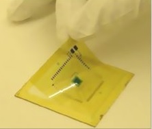
Flexible and stretchable circuit technologies offer reduced volume and weight, increased electrical performance, larger design freedom and improved interconnect reliability. All of these advantages are appealing for space applications. In this paper, two example technologies, the ultra-thin chip package (UTCP) and stretchable moulded interconnect (SMI), are described. The UTCP technology results in a 60μm thick chip package, including the embedding of a 20 μm thick chip, laser or protolithic via definition to the chip contacts and application of fan-out metallization. Imec’s stretchable interconnect technology is inspired by conventional rigid and flexible printed circuit board (PCB) technology. Stretchable interconnects are realized by copper meanders supported by a flexible material (e.g., polyimide). Elastic materials, predominantly silicone rubbers, are used to embed the conductors and the components, thus serving as circuit carrier. The possible advantages of these technologies with respect to space applications are discussed.
The driving application for flexible and stretchable circuit technologies is consumer electronics, especially handheld and mobile devices, which benefit the most from the reduction in form factor, the increased functional density and enlarged user comfort that is made possible with these technologies. Reduced volume and weight, increased electrical performance, larger design freedom and improved interconnect reliability are benefits that are also appealing for space applications.
Traditionally, electronics and sensor circuits are fabricated on flat rigid substrates, like FR-4 PCBs. In this conventional technology, packaged integrated circuits (ICs) and passive components are assembled onto the rigid PCB by soldering. For many applications, especially for mobile, portable, wearable and implantable electronics, the circuit should preferably be seamlessly integrated into the object that is used for transportation, is carried along, or worn on or inside the body. The electronics should be comfortable and unnoticeable to the user. In general, standard circuits do not fulfil these requirements. The user comfort can be increased in two ways. Extreme miniaturisation of the circuit reduces the presence of the system. A second approach is to transform the flat rigid circuit into a three-dimensional, conformable variant, following the random shape of the object or body part onto which it is integrated.
In this contribution, two original technologies developed at imec-CMST are presented. The ultra-thin chip package (UTCP) technology embeds 20–30 μm thick chips in a stack of spin-on polyimide (PI) layers. Adding thinfilm, fan-out metallization results in an extremely miniaturized, lightweight and flexible chip package with a total thickness below 100μm. Next to flexible electronics, a number of technologies for dynamically or one-time deformable stretchable circuits are under development. The stretchable concept is based on the interconnection of individual components or component islands with meander shaped metal wirings and embedding in elastic polymers like silicone rubbers (PDMS), polyurethanes (PU) or other plastics.
Editor's Note: This article originally appeared in the June 2015 issue of The PCB Magazine.
Share on:


Testimonial
"The I-Connect007 team is outstanding—kind, responsive, and a true marketing partner. Their design team created fresh, eye-catching ads, and their editorial support polished our content to let our brand shine. Thank you all! "
Sweeney Ng - CEE PCBSuggested Items
SINBON Celebrates Opening of New US Manufacturing Facility
08/21/2025 | PRNewswireLeading electronics system integrator SINBON Electronics Co., Ltd. held an opening ceremony on August 18 to celebrate its new 59,000-square-foot facility in Clayton, Ohio.
PEDC Call for Abstracts Deadline Extended to Aug. 31
08/20/2025 | I-Connect007 Editorial TeamThe second Pan-European Electronics Design Conference (PEDC) will take place Jan. 21-22, 2026, in Prague, Czech Republic. The call for abstracts deadline has been extended to Aug. 31. Organized jointly by the German Electronics Design and Manufacturing Association (FED) and the Global Electronics Association (formerly IPC), PEDC serves as a European platform for knowledge exchange, networking, and innovation in electronics design and development.
Nano Silver Inks Market Forecast Report 2025-2030
08/20/2025 | Globe NewswireThe Nano Silver Inks Market is expected to grow from USD 427.415 million in 2025 to USD 836.160 million in 2030, at a CAGR of 14.36%.
VVDN Expands Manufacturing Footprint into the UAE to Meet Global Demand
08/20/2025 | PRNewswireVVDN Technologies, a global provider of software, product engineering and electronics manufacturing services & solutions, today announced it is setting up a new manufacturing facility in the UAE as part of its global expansion strategy.
Kimball Electronics Veterans ERG Members Proudly Participate in the 5th Annual Honor and Remember Run
08/20/2025 | Kimball ElectronicsVeterans and Military Service Advocacy (VMSA) Employee Resource Group (ERG) members Michael Mosher (Database Administration Engineer), Michael Stone (Test Technician Team Lead), and Joshua Belcher (Application Development Manager) took part in the 5th Annual Honor & Remember Run, a meaningful event dedicated to honoring fallen service members. The race featured a powerful memorial wall constructed from dog tags.