


 The Marketing Minute: Cracking the Code of Technical Marketing
 Trouble in Your Tank: Implementing Direct Metallization in Advanced Substrate Packaging


Flexible Phase-change Random Access Memory
June 22, 2015 | KAISTEstimated reading time: 2 minutes
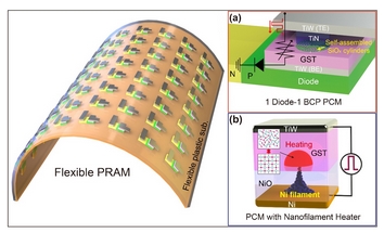
Phase change random access memory (PRAM) is one of the strongest candidates for next-generation nonvolatile memory for flexible and wearable electronics. In order to be used as a core memory for flexible devices, the most important issue is reducing high operating current. The effective solution is to decrease cell size in sub-micron region as in commercialized conventional PRAM. However, the scaling to nano-dimension on flexible substrates is extremely difficult due to soft nature and photolithographic limits on plastics, thus practical flexible PRAM has not been realized yet.
Recently, a team led by Professors Keon Jae Lee and Yeon Sik Jung of the Department of Materials Science and Engineering at KAIST has developed the first flexible PRAM enabled by self-assembled block copolymer (BCP) silica nanostructures with an ultralow current operation (below one quarter of conventional PRAM without BCP) on plastic substrates. BCP is the mixture of two different polymer materials, which can easily create self-ordered arrays of sub-20 nm features through simple spin-coating and plasma treatments. BCP silica nanostructures successfully lowered the contact area by localizing the volume change of phase-change materials and thus resulted in significant power reduction. Furthermore, the ultrathin silicon-based diodes were integrated with phase-change memories (PCM) to suppress the inter-cell interference, which demonstrated random access capability for flexible and wearable electronics. Their work was published in the March issue of ACS Nano: "Flexible One Diode-One Phase Change Memory Array Enabled by Block Copolymer Self-Assembly."
Another way to achieve ultralow-powered PRAM is to utilize self-structured conductive filaments (CF) instead of the resistor-type conventional heater. The self-structured CF nanoheater originated from unipolar memristor can generate strong heat toward phase-change materials due to high current density through the nanofilament. This ground-breaking methodology shows that sub-10 nm filament heater, without using expensive and non-compatible nanolithography, achieved nanoscale switching volume of phase change materials, resulted in the PCM writing current of below 20 uA, the lowest value among top-down PCM devices. This achievement was published in the June online issue of ACS Nano: "Self-Structured Conductive Filament Nanoheater for Chalcogenide Phase Transition." In addition, due to self-structured low-power technology compatible to plastics, the research team has recently succeeded in fabricating a flexible PRAM on wearable substrates.
Professor Lee said, "The demonstration of low power PRAM on plastics is one of the most important issues for next-generation wearable and flexible non-volatile memory. Our innovative and simple methodology represents the strong potential for commercializing flexible PRAM."
In addition, he wrote a review paper regarding the nanotechnology-based electronic devices in the June online issue of Advanced Materials entitled "Performance Enhancement of Electronic and Energy Devices via Block Copolymer Self-Assembly."
Share on:


Testimonial
"The I-Connect007 team is outstanding—kind, responsive, and a true marketing partner. Their design team created fresh, eye-catching ads, and their editorial support polished our content to let our brand shine. Thank you all! "
Sweeney Ng - CEE PCBSuggested Items
Curing and Verification in PCB Shadow Areas
09/17/2025 | Doug Katze, DymaxDesign engineers know a simple truth that often complicates electronics manufacturing: Light doesn’t go around corners. In densely populated PCBs, adhesives and coatings often fail to fully cure in shadowed regions created by tall ICs, connectors, relays, and tight housings.
Marcy’s Musings: Advancing the Advanced Materials Discussion
09/17/2025 | Marcy LaRont -- Column: Marcy's MusingsAs the industry’s most trusted global source of original content about the electronics supply chain, we continually ask you about your concerns, what you care about, and what you most want to learn about. Your responses are insightful and valuable. Thank you for caring enough to provide useful feedback and engage in dialogue.
September 2025 PCB007 Magazine: The Future of Advanced Materials
09/16/2025 | I-Connect007 Editorial TeamMoore’s Law is no more, and the advanced material solutions being developed to grapple with this reality are surprising, stunning, and perhaps a bit daunting. Buckle up for a dive into advanced materials and a glimpse into the next chapters of electronics manufacturing.
I-Connect007 Launches Advanced Electronics Packaging Digest
09/15/2025 | I-Connect007I-Connect007 is pleased to announce the launch of Advanced Electronics Packaging Digest (AEPD), a new monthly digital newsletter dedicated to one of the most critical and rapidly evolving areas of electronics manufacturing: advanced packaging at the interconnect level.
Panasonic Industry will Double the Production Capacity of MEGTRON Multi-layer Circuit Board Materials Over the Next Five Years
09/15/2025 | Panasonic Industry Co., Ltd.Panasonic Industry Co., Ltd., a Panasonic Group company, announced plans for a major expansion of its global production capacity for MEGTRON multi-layer circuit board materials today. The company plans to double its production over the next five years to meet growing demand in the AI server and ICT infrastructure markets.