


 The Marketing Minute: Cracking the Code of Technical Marketing
 Trouble in Your Tank: Implementing Direct Metallization in Advanced Substrate Packaging


Sweeping Lasers Snap Together Nanoscale Geometric Grids
June 24, 2015 | Brookhaven National LaboratoryEstimated reading time: 3 minutes
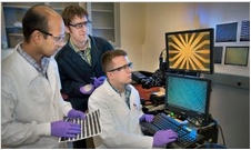
Down at the nanoscale, where objects span just billionths of a meter, the size and shape of a material can often have surprising and powerful electronic and optical effects. Building larger materials that retain subtle nanoscale features is an ongoing challenge that shapes countless emerging technologies.
Now, scientists at the U.S. Department of Energy's Brookhaven National Laboratory have developed a new technique to rapidly create nano-structured grids for functional materials with unprecedented versatility.
"We can fabricate multi-layer grids composed of different materials in virtually any geometric configuration," said study coauthor and Brookhaven Lab scientist Kevin Yager. "By quickly and independently controlling the nanoscale structure and the composition, we can tailor the performance of these materials. Crucially, the process can be easily adapted for large-scale applications."
The results—published online June 23 in the journal Nature Communications—could transform the manufacture of high-tech coatings for anti-reflective surfaces, improved solar cells, and touchscreen electronics.
The scientists synthesized the materials at Brookhaven Lab's Center for Functional Nanomaterials(CFN) and characterized the nanoscale architectures using electron microscopy at CFN and x-ray scattering at the National Synchrotron Light Source—both DOE Office of Science User Facilities.
The new technique relies on polymer self-assembly, where molecules are designed to spontaneously assemble into desired structures. Self-assembly requires a burst of heat to make the molecules snap into the proper configurations. Here, an intensely hot laser swept across the sample to transform disordered polymer blocks into precise arrangements in just seconds.
"Self-assembled structures tend to automatically follow molecular preferences, making custom architectures challenging," said lead author Pawel Majewski, a postdoctoral researcher at Brookhaven. "Our laser technique forces the materials to assemble in a particular way. We can then build structures layer-by-layer, constructing lattices composed of squares, rhombuses, triangles, and other shapes."
For the first step in grid construction, the team took advantage of their recent invention of laser zone annealing (LZA) to produce the extremely localized thermal spikes needed to drive ultra-fast self-assembly.
To further exploit the power and precision of LZA, the researchers applied a heat-sensitive elastic coating on top of the unassembled polymer film. The sweeping laser's heat causes the elastic layer to expand—like shrink-wrap in reverse—which pulls and aligns the rapidly forming nanoscale cylinders.
"The end result is that in less than one second, we can create highly aligned batches of nano-cylinders," said study coauthor Charles Black, who leads the Electronic Nanomaterials group at CFN. "This order persists over macroscopic areas and would be difficult to achieve with any other method."
To make these two-dimensional grids functional, the scientists converted the polymer base into other materials.
One method involved taking the nano-cylinder layer and dipping it into a solution containing metal salts. These molecules then glom onto the self-assembled polymer, converting it into a metallic mesh. A wide range of reactive or conductive metals can be used, including platinum, gold, and palladium.
They also used a technique called vapor deposition, where a vaporized material infiltrates the polymer nano-cylinders and transforms them into functional nano-wires.
Layer-by-layer lattice
The first completed nano-wire array acts as the foundation of the full lattice. Additional layers, each one following variations on that same process, are then stacked to produce customized, crisscrossing configurations—like chain-link fences 10,000 times thinner than a human hair.
"The direction of the laser sweeping across each unassembled layer determines the orientation of the nano-wire rows," Yager said. "We shift that laser direction on each layer, and the way the rows intersect and overlap shapes the grid. We then apply the functional materials after each layer forms. It's an exceptionally fast and simple way to produce such precise configurations."
Study coauthor Atikur Rahman, a CFN postdoctoral researcher, added, "We can stack metals on insulators, too, embedding different functional properties and interactions within one lattice structure.
"The size and the composition of the mesh make a huge difference," Rahman continued. "For example, a single layer of platinum nano-wires conducts electricity in only one direction, but a two-layer mesh conducts uniformly in all directions."
LZA is precise and powerful enough to overcome interface interactions, allowing it to drive polymer self-assembly even on top of complex underlying layers. This versatility enables the use of a wide variety of materials in different nanoscale configurations.
"We can generate nearly any two-dimensional lattice shape, and thus have a lot of freedom in fabricating multi-component nanostructures," Yager said. "It's hard to anticipate all the technologies this rapid and versatile technique will allow."
Brookhaven National Laboratory is supported by the Office of Science of the U.S. Department of Energy. The Office of Science is the single largest supporter of basic research in the physical sciences in the United States, and is working to address some of the most pressing challenges of our time. For more information, please visit science.energy.gov.
Share on:


Testimonial
"In a year when every marketing dollar mattered, I chose to keep I-Connect007 in our 2025 plan. Their commitment to high-quality, insightful content aligns with Koh Young’s values and helps readers navigate a changing industry. "
Brent Fischthal - Koh YoungSuggested Items
Curing and Verification in PCB Shadow Areas
09/17/2025 | Doug Katze, DymaxDesign engineers know a simple truth that often complicates electronics manufacturing: Light doesn’t go around corners. In densely populated PCBs, adhesives and coatings often fail to fully cure in shadowed regions created by tall ICs, connectors, relays, and tight housings.
Marcy’s Musings: Advancing the Advanced Materials Discussion
09/17/2025 | Marcy LaRont -- Column: Marcy's MusingsAs the industry’s most trusted global source of original content about the electronics supply chain, we continually ask you about your concerns, what you care about, and what you most want to learn about. Your responses are insightful and valuable. Thank you for caring enough to provide useful feedback and engage in dialogue.
September 2025 PCB007 Magazine: The Future of Advanced Materials
09/16/2025 | I-Connect007 Editorial TeamMoore’s Law is no more, and the advanced material solutions being developed to grapple with this reality are surprising, stunning, and perhaps a bit daunting. Buckle up for a dive into advanced materials and a glimpse into the next chapters of electronics manufacturing.
I-Connect007 Launches Advanced Electronics Packaging Digest
09/15/2025 | I-Connect007I-Connect007 is pleased to announce the launch of Advanced Electronics Packaging Digest (AEPD), a new monthly digital newsletter dedicated to one of the most critical and rapidly evolving areas of electronics manufacturing: advanced packaging at the interconnect level.
Panasonic Industry will Double the Production Capacity of MEGTRON Multi-layer Circuit Board Materials Over the Next Five Years
09/15/2025 | Panasonic Industry Co., Ltd.Panasonic Industry Co., Ltd., a Panasonic Group company, announced plans for a major expansion of its global production capacity for MEGTRON multi-layer circuit board materials today. The company plans to double its production over the next five years to meet growing demand in the AI server and ICT infrastructure markets.