


 The Marketing Minute: Cracking the Code of Technical Marketing
 Trouble in Your Tank: Implementing Direct Metallization in Advanced Substrate Packaging


New 2-D Material's Properties Show Potential
June 24, 2015 | University of Nebraska–LincolnEstimated reading time: 3 minutes
One completed a series of theoretical calculations to predict its properties with the help of a massive computing center. The other grew it in bulk before waxing its atom-thin whiskers with the assistance of adhesive tape.
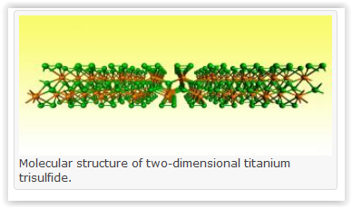
Together, University of Nebraska-Lincoln chemists Xiao Cheng Zeng and Alexander Sinitskii have demonstrated that a compound called titanium trisulfide could surge toward the fore of two-dimensional materials that are gaining popularity among designers of microelectronics.
The rise of 2-D materials -- sheets no more than a few atoms thick -- began with the 2004 demonstration of graphene, which remains the strongest and thinnest material known.
Zeng and Sinitskii have published two recent studies showing that titanium trisulfide compares favorably not only with graphene, but also phosphorene and molybdenum disulfide -- fellow 2-D materials that have shown great promise for electronic applications.
"There was no interest in the properties of few-layer titanium trisulfide until now," said Zeng, an Ameritas University Professor of chemistry. "We were among the first to look at them, and we've been very excited by what we've seen."
Zeng's theoretical study revealed that 2-D titanium trisulfide has the potential to transport electrons faster than phosphorene and molybdenum disulfide. This "electron mobility" helps dictate the speed of transistors, the devices that control electric current and amplify electrical power in technology ranging from cellphones to spacecraft.
Transistors also form the core of semiconductors, which rapidly switch between a current-conducting "on" state and current-insulating "off" state to represent the 1s and 0s of digital computing.
Graphene boasts unparalleled conductivity, but crucially lacks the quality that can turn it off: a band gap, which describes the energy necessary for electrons to jump from their near orbits around atoms to an outer "conduction band" that promotes conductivity.
Zeng and Sinitskii found that titanium trisulfide has a moderate band gap that approximates the one found in semiconductor favorite silicon, making it ideal for the on/off switching prized in such devices. The material also yields a large disparity between "on" and "off" conditions, which helps distinguish between resulting 1s and 0s.
The material's band gap also allows it to absorb elementary particles of light known as photons from most of the sun's emission spectrum. Because of this, titanium trisulfide could also prove useful in solar-cell designs, Sinitskii said.
Sinitskii, an assistant professor of chemistry, followed up on Zeng's theoretical calculations by combining titanium and sulfur to form a block of titanium trisulfide. He then used adhesive tape to rip off microscopic whiskers of the compound in the same way that the pioneers of graphene did with graphite more than a decade ago.
Sinitskii turned those whiskers into transistors and directed the performance tests that confirmed his colleague's work.
"As a theoretician, I always want to predict something," Zeng said. "The dream for us is that somebody makes it in the laboratory.
"I couldn't help but tell Alex. He's one of the leading experts in the world when it comes to making two-dimensional materials, and he did it just a couple of months after (I asked him)."
Sinitskii said the 2-D predecessors of titanium trisulfide should help accelerate his team's efforts to study and improve it.
"When people started working with devices based on graphene, the first two-dimensional material, everything was new," he said. "Researchers studied how different parameters affect device performance. When they started working on other 2-D materials, the knowledge generated from graphene research was very useful.
"In our case, we're actually in quite a good position, because we can learn a lot from those earlier studies and apply prior knowledge to making better transistors from titanium trisulfide."
Zeng's recent study, published in the journal Angewandte Chemie International Edition, was co-authored with postdoctoral researcher Jun Dai. The researchers performed their calculations through UNL's Holland Computing Center.
The Sinitskii-led study appeared in the journal Nanoscale. He shared authorship with postdoctoral researcher Alexey Lipatov and graduate students Peter Wilson, Mikhail Shekhirev, Jacob Teeter and Ross Netusil.
Both research teams received support from UNL's Materials Research Science and Engineering Center, part of a nationwide network of MRSECs sponsored by the National Science Foundation. They conducted their work in conjunction with the Nebraska Center for Materials and Nanoscience.
Share on:


Testimonial
"The I-Connect007 team is outstanding—kind, responsive, and a true marketing partner. Their design team created fresh, eye-catching ads, and their editorial support polished our content to let our brand shine. Thank you all! "
Sweeney Ng - CEE PCBSuggested Items
Curing and Verification in PCB Shadow Areas
09/17/2025 | Doug Katze, DymaxDesign engineers know a simple truth that often complicates electronics manufacturing: Light doesn’t go around corners. In densely populated PCBs, adhesives and coatings often fail to fully cure in shadowed regions created by tall ICs, connectors, relays, and tight housings.
Marcy’s Musings: Advancing the Advanced Materials Discussion
09/17/2025 | Marcy LaRont -- Column: Marcy's MusingsAs the industry’s most trusted global source of original content about the electronics supply chain, we continually ask you about your concerns, what you care about, and what you most want to learn about. Your responses are insightful and valuable. Thank you for caring enough to provide useful feedback and engage in dialogue.
September 2025 PCB007 Magazine: The Future of Advanced Materials
09/16/2025 | I-Connect007 Editorial TeamMoore’s Law is no more, and the advanced material solutions being developed to grapple with this reality are surprising, stunning, and perhaps a bit daunting. Buckle up for a dive into advanced materials and a glimpse into the next chapters of electronics manufacturing.
I-Connect007 Launches Advanced Electronics Packaging Digest
09/15/2025 | I-Connect007I-Connect007 is pleased to announce the launch of Advanced Electronics Packaging Digest (AEPD), a new monthly digital newsletter dedicated to one of the most critical and rapidly evolving areas of electronics manufacturing: advanced packaging at the interconnect level.
Panasonic Industry will Double the Production Capacity of MEGTRON Multi-layer Circuit Board Materials Over the Next Five Years
09/15/2025 | Panasonic Industry Co., Ltd.Panasonic Industry Co., Ltd., a Panasonic Group company, announced plans for a major expansion of its global production capacity for MEGTRON multi-layer circuit board materials today. The company plans to double its production over the next five years to meet growing demand in the AI server and ICT infrastructure markets.