


 The Marketing Minute: Cracking the Code of Technical Marketing
 Trouble in Your Tank: Implementing Direct Metallization in Advanced Substrate Packaging


Towards Graphene Biosensors
June 25, 2015 | Helmholtz Zentrum BerlinEstimated reading time: 2 minutes
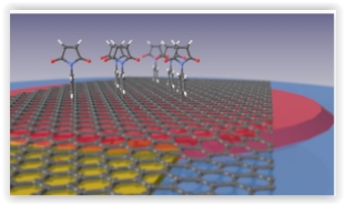
For the first time, a team of scientists has succeeded in precisely measuring and controlling the thickness of an organic compound that has been bound to a graphene layer. This might enable graphene to be used as a sensitive detector for biological molecules in the future.
Pure carbon occurs in many forms. Besides the classical configurations found in diamonds, graphite, and coal, there are other younger exotic cousins such as graphene. Its structure resembles a honeycomb – a hexagonal mesh with a carbon atom at every corner – that is only a single atomic layer thick. Hence, it is essentially two-dimensional. As a result, graphene is extremely conductive, completely transparent, and quite resilient both chemically and mechanically.
Graphene is not very selective
It has long been known that graphene is also fundamentally suited to detecting traces of organic molecules. This is because the electrical conductivity of graphene drops as soon as foreign molecules bind to it. The problem, though, is that this happens with almost every molecule. Graphene is not very selective, which makes it very difficult to differentiate molecules. Therefore, it cannot be used as a sensor.
Now, mounting brackets for detector molecules attached
Now a team from the HZB Institute for Silicon Photovoltaics has found a way to increase the selectivity. They were successful in electrochemically activating graphene and preparing it to host molecules that act as selective binding sites. To accomplish this, para-maleimidophenyl groups from an organic solution were grafted to the surface of the graphene. These organic molecules behave like mounting brackets to which the selective detector molecules can be attached in the next step. “Thanks to these molecules, the graphene can now be employed for detecting various substances similar to how a key fits a lock”, explains Dr. Marc Gluba. The “lock” molecules on the surface are highly selective and only absorb the matching “key” molecules.
Large graphene surfaces at HZB
Other research groups had also carried out experiments along these lines. However, they only had tiny graphene flakes with diameters in the microns available to them, so that edge effects predominated. Meanwhile, physicists and chemists at HZB produced graphene surfaces several square centimeters in size so that edge effects play hardly any role in comparison to the surface processes. Then, they transferred the graphene layer to a quartz crystal microbalance. Any increase in mass alters the oscillatory frequency of the quartz crystal that even small amounts right down to individual molecular layers can be measured.
Precise detection and control
“For the first time, we were able to precisely and accurately detect how many molecules actually were grafted to the surface of the graphene”, reports junior researcher Felix Rösicke, who investigated this problem for his doctoral dissertation. “In addition, we can precisely control how many molecules bind to the graphene by adjusting an applied voltage”, explains Dr. Jörg Rappich from the HZB Institute for Silicon Photovoltaics, Rösicke’s advisor.
“The hopes we have for graphene are really enormous”, says Prof. Norbert Nickel, head of the research team. For example, one thing you could imagine would be a really inexpensive "lab-on-a-chip” – you would apply a single drop of blood and immediately obtain data for important medical diagnostics.
Share on:


Testimonial
"In a year when every marketing dollar mattered, I chose to keep I-Connect007 in our 2025 plan. Their commitment to high-quality, insightful content aligns with Koh Young’s values and helps readers navigate a changing industry. "
Brent Fischthal - Koh YoungSuggested Items
Driving Innovation: Depth Routing Processes—Achieving Unparalleled Precision in Complex PCBs
09/08/2025 | Kurt Palmer -- Column: Driving InnovationIn PCB manufacturing, the demand for increasingly complex and miniaturized designs continually pushes the boundaries of traditional fabrication methods, including depth routing. Success in these applications demands not only on robust machinery but also sophisticated control functions. PCB manufacturers rely on advanced machine features and process methodologies to meet their precise depth routing goals. Here, I’ll explore some crucial functions that empower manufacturers to master complex depth routing challenges.
Polar Instruments Announces Additive Transmission Line Support for Si9000e
08/20/2025 | Polar InstrumentsTransmission lines embedded into the PCB surface are a feature of UHDI constructions. The 2025 fall release of Polar's Si9000e PCB impedance & insertion loss transmission line field solver incorporates eight new single ended, differential and coplanar transmission line structures.
Henniker Plasma Launches Stratus Turnkey Plasma Manufacturing Cell
08/13/2025 | Henniker PlasmaHenniker Plasma, a leading manufacturer of plasma treatment systems, proudly announces the launch of its Stratus Plasma Manufacturing Cell range — a fully integrated, turnkey solution that combines advanced atmospheric plasma surface treatment with robotic automation.
Trouble in Your Tank: Metallizing Flexible Circuit Materials—Mitigating Deposit Stress
08/04/2025 | Michael Carano -- Column: Trouble in Your TankMetallizing materials, such as polyimide used for flexible circuitry and high-reliability multilayer printed wiring boards, provide a significant challenge for process engineers. Conventional electroless copper systems often require pre-treatments with hazardous chemicals or have a small process window to achieve uniform coverage without blistering. It all boils down to enhancing the adhesion of the thin film of electroless copper to these smooth surfaces.
Designers Notebook: Basic PCB Planning Criteria—Establishing Design Constraints
07/22/2025 | Vern Solberg -- Column: Designer's NotebookPrinted circuit board development flows more smoothly when all critical issues are predefined and understood from the start. As a basic planning strategy, the designer must first consider the product performance criteria, then determine the specific industry standards or specifications that the product must meet. Planning also includes a review of all significant issues that may affect the product’s manufacture, performance, reliability, overall quality, and safety.