


 The Marketing Minute: Cracking the Code of Technical Marketing
 Trouble in Your Tank: Implementing Direct Metallization in Advanced Substrate Packaging


Ultrasonic Fingerprint Sensor May Take Smartphone Security to New Level
June 29, 2015 | AIP.orgEstimated reading time: 3 minutes
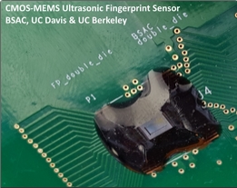
Fingerprint sensor technology currently used in smartphones like the iPhone 6 produces a two-dimensional image of a finger’s surface, which can be spoofed fairly easily with a printed image of the fingerprint. A newly developed ultrasonic sensor eliminates that risk by imaging the ridges and valleys of the fingerprint’s surface, and the tissue beneath, in three dimensions.
“Using passwords for smartphones was a big security problem, so we anticipated that a biometric solution was ahead,” said David A. Horsley, a professor of mechanical and aerospace engineering at the University of California, Davis. He is a director of the Berkeley Sensor and Actuator Center, which is located on the campuses of UC Davis and the University of California, Berkeley and is co-directed by Professor Bernhard Boser at UC Berkeley.
“After Apple announced a fingerprint sensor in their new iPhone in 2013, it was inevitable that more would follow," said Horsley. He and his colleagues describe their new technology this week, in a story appearing on the cover of the journal Applied Physics Letters, from AIP Publishing.
The origins of the new technology began to come together in 2007, when the teams at the Berkeley Sensor and Actuator Center collaborated to initiate research into piezoelectric-micromachined ultrasonic transducers (PMUTs).
“We developed arrays of PMUTs, along with a custom application-specific integrated circuit (ASIC) and the supporting electronics,” Horsley said. “Our work was so successful that we spun off Chirp Microsystems, in 2013, to commercialize it.” Shortly before then, in 2011, while exploring other uses for their PMUT technology, they quickly realized that fingerprint sensing was an ideal fit.
"Luckily, we recruited a group of exceptional students to realize our vision, as well as partners within the industry—our co-authors at InvenSense Inc. and a few other companies—who funded the work and fabricated our designs," Horsley said.
The basic concepts behind the researchers’ technology are akin to those of medical ultrasound imaging. They created a tiny ultrasound imager, designed to observe only a shallow layer of tissue near the finger’s surface. “Ultrasound images are collected in the same way that medical ultrasound is conducted,” said Horsley. “Transducers on the chip’s surface emit a pulse of ultrasound, and these same transducers receive echoes returning from the ridges and valleys of your fingerprint’s surface.”
An ultrasonic fingerprint sensor measures a three-dimensional, volumetric image of the finger’s surface and the tissues beneath—making it difficult to “spoof” or fake.Credit-Dave Horsley/UC-Davis
The basis for the ultrasound sensor is an array of MEMS ultrasound devices with highly uniform characteristics, and therefore very similar frequency response characteristics (see video).
To fabricate their imager, the group employed existing microelectromechanical systems (MEMS) technology, which smartphones rely on for such functions as microphones and directional orientation. They used a modified version of the manufacturing process used to make the MEMS accelerometer and gyroscope found in the iPhone and many other consumer electronics devices.
“Our chip is fabricated from two wafers—a MEMS wafer that contains the ultrasound transducers and a CMOS wafer that contains the signal processing circuitry,” explained Horsley. “These wafers are bonded together, then the MEMS wafer is ‘thinned’ to expose the ultrasound transducers.” (CMOS, or complementary metal–oxide–semiconductor, is the silicon-based technology used to make transistors in microchips.)
Horsley's group views ultrasound as the next frontier for MEMS technology. “Because we were able to use low-cost, high-volume manufacturing processes that produce hundreds of millions of MEMS sensors for consumer electronics each year, our ultrasound chips can be manufactured at an extremely low cost,” he said.
The imager is powered by a 1.8-Volt power supply, using a power-efficient charge pump on their ASIC or application-specific integrated circuit. “Our ultrasound transducers have high sensitivity and the receiver electronics are located directly beneath the array, which results in low electrical parasitics,” Horsley noted. “Using low-voltage integrated circuits will reduce the cost of our sensor and open up myriad new applications where the cost, size, and power consumption of existing ultrasound sensors are currently prohibitive.”
Within the realm of biometrics and information security, the group’s work is particularly significant, Horsley said. “Our ultrasonic fingerprint sensors have the ability to measure a three-dimensional, volumetric image of the finger surface and the tissues beneath the surface—making fingerprint sensors more robust and secure.”
Beyond biometrics and information security purposes, the new technology is expected to find many other applications, including “low-cost ultrasound as a medical diagnostic tool or for personal health monitoring,” he added.
Share on:


Testimonial
"Advertising in PCB007 Magazine has been a great way to showcase our bare board testers to the right audience. The I-Connect007 team makes the process smooth and professional. We’re proud to be featured in such a trusted publication."
Klaus Koziol - atgSuggested Items
Nortech Systems Achieves Enhanced Fiber Optic Performance
09/16/2025 | Nortech SystemsNortech Systems Incorporated, a leading provider of design and manufacturing solutions for complex electromedical devices and electromechanical systems, announced significant advancements in its fiber optic capabilities.
Altair, Wichita State University’s NIAR Sign MoU to Accelerate Aerospace Innovation
09/16/2025 | AltairAltair, a global leader in computational intelligence, and Wichita State University’s (WSU) National Institute for Aviation Research (NIAR), one of the world’s leading aerospace research institutions, have signed a memorandum of understanding (MoU) to advance innovation across the aerospace and defense industries.
India’s Aerospace and Defence Engineered for Power, Driven by Electronics
09/16/2025 | Gaurab Majumdar, Global Electronics AssociationWith a defence budget of $82.05 billion (2025–26) and a massive $223 billion earmarked for aerospace and defence spending over the next decade, India is rapidly positioning itself as a major player in the global defence and aerospace market.
Honeywell-Led Consortium Receives UK Government Funding to Revolutionize Aerospace Manufacturing
09/02/2025 | HoneywellA consortium led by Honeywell has received UK Government funding for a project that aims to revolutionize how critical aerospace technologies are manufactured in the UK through the use of AI and additive manufacturing.
Coherent Announces Agreement to Sell Aerospace and Defense Business to Advent for $400 Million
08/15/2025 | AdventCoherent Corp., a global leader in photonics, today announced that it has entered into a definitive agreement to sell its Aerospace and Defense business to Advent, a leading global private equity investor, for $400 million. Proceeds will be used to reduce debt, which will be immediately accretive to Coherent’s EPS.