


 The Marketing Minute: Cracking the Code of Technical Marketing
 Trouble in Your Tank: Implementing Direct Metallization in Advanced Substrate Packaging


Making New Materials with Micro-explosions
June 30, 2015 | Australian National UniversityEstimated reading time: 2 minutes
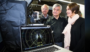
Scientists have made exotic new materials by creating laser-induced micro-explosions in silicon, the common computer chip material.
The new technique could lead to the simple creation and manufacture of superconductors or high-efficiency solar cells and light sensors, said leader of the research, Professor Andrei Rode, from The Australian National University (ANU).
"We've created two entirely new crystal arrangements, or phases, in silicon and seen indications of potentially four more," said Professor Rode, a laser physicist at the ANU Research School of Physics and Engineering (RSPE).
"Theory predicts these materials could have very interesting electronic properties, such as an altered band gap, and possibly superconductivity if properly doped."
By focusing lasers onto silicon buried under a clear layer of silicon dioxide, the group have perfected a way to reliably blast tiny cavities in the solid silicon. This creates extremely high pressure around the explosion site and forms the new phases.
The phases have complex structures, which took the team of physicists from ANU and University College London a year to understand.
Using a combination of electron diffraction patterns and structure predictions, the team discovered the new materials have crystal structures that repeat every 12, 16 or 32 atoms respectively, said Professor Jim Williams, from the Electronic Material Engineering group at RSPE.
"The micro-explosions change silicon's simplicity to much more complex structures, which opens up possibility for unusual and unexpected properties," he said.
These complex phases are often unstable, but the small size of the structures means the materials cool very quickly and solidify before they can decay, said Professor Eugene Gamaly, also from the ANU Research School of Physics and Engineering. The new crystal structures have survived for more than a year now.
"These new discoveries are not an accident, they are guided by a deep understanding of how lasers interact with matter," he said.
Conventional methods for creating materials with high pressure use tiny diamond anvils to poke or squeeze materials. However, the ultra-short laser micro-explosions create pressures many times higher than the strength of diamond crystal can produce.
The team's new method promises a much cheaper and industrially-friendly method for large scale manufacturing of these exotic materials, says Dr Jodie Bradby, also from ANU Research School of Physics and Engineering.
"We reliably create thousands of micron-size modified zones in normal silicon within a second," she said.
"The semiconductor industry is a multi-billion dollar operation - even a small change in the position of a few silicon atoms has the potential to have a major impact."
Share on:


Testimonial
"Advertising in PCB007 Magazine has been a great way to showcase our bare board testers to the right audience. The I-Connect007 team makes the process smooth and professional. We’re proud to be featured in such a trusted publication."
Klaus Koziol - atgSuggested Items
Curing and Verification in PCB Shadow Areas
09/17/2025 | Doug Katze, DymaxDesign engineers know a simple truth that often complicates electronics manufacturing: Light doesn’t go around corners. In densely populated PCBs, adhesives and coatings often fail to fully cure in shadowed regions created by tall ICs, connectors, relays, and tight housings.
Marcy’s Musings: Advancing the Advanced Materials Discussion
09/17/2025 | Marcy LaRont -- Column: Marcy's MusingsAs the industry’s most trusted global source of original content about the electronics supply chain, we continually ask you about your concerns, what you care about, and what you most want to learn about. Your responses are insightful and valuable. Thank you for caring enough to provide useful feedback and engage in dialogue.
September 2025 PCB007 Magazine: The Future of Advanced Materials
09/16/2025 | I-Connect007 Editorial TeamMoore’s Law is no more, and the advanced material solutions being developed to grapple with this reality are surprising, stunning, and perhaps a bit daunting. Buckle up for a dive into advanced materials and a glimpse into the next chapters of electronics manufacturing.
I-Connect007 Launches Advanced Electronics Packaging Digest
09/15/2025 | I-Connect007I-Connect007 is pleased to announce the launch of Advanced Electronics Packaging Digest (AEPD), a new monthly digital newsletter dedicated to one of the most critical and rapidly evolving areas of electronics manufacturing: advanced packaging at the interconnect level.
Panasonic Industry will Double the Production Capacity of MEGTRON Multi-layer Circuit Board Materials Over the Next Five Years
09/15/2025 | Panasonic Industry Co., Ltd.Panasonic Industry Co., Ltd., a Panasonic Group company, announced plans for a major expansion of its global production capacity for MEGTRON multi-layer circuit board materials today. The company plans to double its production over the next five years to meet growing demand in the AI server and ICT infrastructure markets.