


 The Marketing Minute: Cracking the Code of Technical Marketing
 Trouble in Your Tank: Implementing Direct Metallization in Advanced Substrate Packaging


Chemists Characterize 3-D Macroporous Hydrogels
July 1, 2015 | Carnegie Mellon UniversityEstimated reading time: 2 minutes
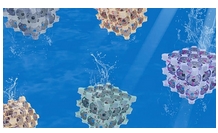
Carnegie Mellon University chemists have developed two novel methods to characterize 3-dimensional macroporous hydrogels — materials that hold great promise for developing “smart” responsive materials that can be used for catalysts, chemical detectors, tissue engineering scaffolds and absorbents for carbon capture.
Researchers working in the lab of Carnegie Mellon Professor Krzysztof Matyjaszewski published their results in the May issue of Advanced Science, with the article featured on the journal’s back cover. Their findings are the latest in Matyjaszewski lab’s long history of breakthroughs in polymer science.
The 3DOM hydrogels contain a network of interconnected pores with uniform size. The configuration of these pores allows the materials to hold a large amount of liquid, and influences the material’s properties.
However, while the materials are easily made using a process called colloidal crystal templating, their nature has made it difficult for scientists to characterize the exact internal structure of the 3DOM hydrogels.
“The porous structure that makes these materials so useful is also what makes them so hard to characterize,” said Hongkun He, a doctoral student in Matyjaszewski’s lab. “The pores can hold large amounts of water, but if you remove this water to study them, the pores collapse and you can’t map them.”
He and his collaborators were able to characterize the 3DOM hydrogels using an indirect electron microscopy method. They soaked the hydrogels in a solution of a crosslinker, which created rigid inverse replicas of the initial 3DOM structures. They then used scanning electron microscopy (SEM) to image the section surfaces of the inverse replicas.
The researchers also found they were able to rehydrate the hydrogels, demonstrating the material’s shape memory properties — properties that are key to creating smart materials.
He also was able to resolve the structure of hydrated 3DOM hydrogels using nanoscale resolution X-ray microscopy (ZEISS Xradia 800 Ultra). This technique, which is noninvasive and nondestructive, allowed the researchers to visualize the hydrogels in 3 dimensions under ambient conditions.
“This marks the first time that we have been able to visualize the reversible porous structure within this material,” said Matyjaszewski, the J.C. Warner University Professor of Natural Sciences. “Well-defined 3DOM hydrogels provide a versatile platform for a wide variety of functional materials.”
The researchers believe that the simple and effective structural characterization methods they developed for the 3DOM hydrogels will advance research into the materials. They have been able to make further chemical modifications to the pores of the 3DOM hydrogels by grafting with organic compounds and polymers. This process will allow them to use the hydrogels as “stem gels” that can evolve into materials with programmed properties and functions, such as responsive materials, organic–inorganic composites and bioactive hydrogels for digestion or separation of bio (macro) molecules.
Additional authors include Shawn Litster, Saadyah Averick, Pratiti Mandal, Hangjun Ding and Sipei Li of Carnegie Mellon, and Jeff Gelb, Naomi Kotwal and Arno Merkle of Carl Zeiss X-Ray Microscopy. Ding also has an appointment at the University of Science and Technology, Beijing.
Share on:


Testimonial
"Advertising in PCB007 Magazine has been a great way to showcase our bare board testers to the right audience. The I-Connect007 team makes the process smooth and professional. We’re proud to be featured in such a trusted publication."
Klaus Koziol - atgSuggested Items
Curing and Verification in PCB Shadow Areas
09/17/2025 | Doug Katze, DymaxDesign engineers know a simple truth that often complicates electronics manufacturing: Light doesn’t go around corners. In densely populated PCBs, adhesives and coatings often fail to fully cure in shadowed regions created by tall ICs, connectors, relays, and tight housings.
Marcy’s Musings: Advancing the Advanced Materials Discussion
09/17/2025 | Marcy LaRont -- Column: Marcy's MusingsAs the industry’s most trusted global source of original content about the electronics supply chain, we continually ask you about your concerns, what you care about, and what you most want to learn about. Your responses are insightful and valuable. Thank you for caring enough to provide useful feedback and engage in dialogue.
September 2025 PCB007 Magazine: The Future of Advanced Materials
09/16/2025 | I-Connect007 Editorial TeamMoore’s Law is no more, and the advanced material solutions being developed to grapple with this reality are surprising, stunning, and perhaps a bit daunting. Buckle up for a dive into advanced materials and a glimpse into the next chapters of electronics manufacturing.
I-Connect007 Launches Advanced Electronics Packaging Digest
09/15/2025 | I-Connect007I-Connect007 is pleased to announce the launch of Advanced Electronics Packaging Digest (AEPD), a new monthly digital newsletter dedicated to one of the most critical and rapidly evolving areas of electronics manufacturing: advanced packaging at the interconnect level.
Panasonic Industry will Double the Production Capacity of MEGTRON Multi-layer Circuit Board Materials Over the Next Five Years
09/15/2025 | Panasonic Industry Co., Ltd.Panasonic Industry Co., Ltd., a Panasonic Group company, announced plans for a major expansion of its global production capacity for MEGTRON multi-layer circuit board materials today. The company plans to double its production over the next five years to meet growing demand in the AI server and ICT infrastructure markets.