


 The Marketing Minute: Cracking the Code of Technical Marketing
 Trouble in Your Tank: Implementing Direct Metallization in Advanced Substrate Packaging


New Method for Cheaper Solar-energy Storage
July 2, 2015 | EPFLEstimated reading time: 2 minutes
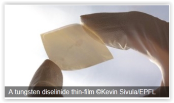
Many different materials have been considered for use in direct solar-to-hydrogen conversion technologies but "2-D materials” have recently been identified as promising candidates. In general these materials—which famously include graphene—have extraordinary electronic properties. However, harvesting usable amounts of solar energy requires large areas of solar panels, and it is notoriously difficult and expensive to fabricate thin films of 2-D materials at such a scale and maintain good performance.
Kevin Sivula and colleagues at EPFL addressed this problem with an innovative and cheap method that uses the boundary between two non-mixing liquids. The researchers focused on one of the best 2-D materials for solar water splitting, called “tungsten diselenide”. Past studies have shown that this material has a great efficiency for converting solar energy directly into hydrogen fuel while also being highly stable.
Before making a thin film of it, the scientists first had to achieve an even dispersion of the material. To do this, they mixed the tungsten diselenide powder with a liquid solvent using sonic vibrations to “exfoliate” it into thin, 2-D flakes, and then added special chemicals to stabilize the mix. Developed by Sivula’s lab (2014), this technique produces an even dispersion of the flakes that is similar to an ink or a paint.
The researchers then used an out-of-the-box innovation to produce high-quality thin films: they injected the tungsten diselenide ink at the boundary between two liquids that do not mix. Exploiting this oil-and-water effect, they used the interface of the two liquids as a “rolling pin” that forced the 2-D flakes to form an even and high-quality thin film with minimal clumping and restacking. The liquids were then carefully removed and the thin film was transferred to a flexible plastic support, which is much less expensive than a traditional solar panel.
The thin film produced like this was tested and found to be superior in efficiency to films made with the same material but using other comparable methods. At this proof-of-concept stage, the direct solar-to-hydrogen conversion efficiency was around 1%—already a vast improvement over thin films prepared by other methods, and with considerable potential for higher efficiencies in the future.
More importantly, this liquid-liquid method can be scaled up on a commercial level. “It is suitable for rapid and large-area roll-to-roll processing,” says Kevin Sivula. “Considering the stability of these materials and the comparative ease of our deposition method, this represents an important advance towards economical solar-to-fuel energy conversion.”
Share on:


Testimonial
"The I-Connect007 team is outstanding—kind, responsive, and a true marketing partner. Their design team created fresh, eye-catching ads, and their editorial support polished our content to let our brand shine. Thank you all! "
Sweeney Ng - CEE PCBSuggested Items
Curing and Verification in PCB Shadow Areas
09/17/2025 | Doug Katze, DymaxDesign engineers know a simple truth that often complicates electronics manufacturing: Light doesn’t go around corners. In densely populated PCBs, adhesives and coatings often fail to fully cure in shadowed regions created by tall ICs, connectors, relays, and tight housings.
Marcy’s Musings: Advancing the Advanced Materials Discussion
09/17/2025 | Marcy LaRont -- Column: Marcy's MusingsAs the industry’s most trusted global source of original content about the electronics supply chain, we continually ask you about your concerns, what you care about, and what you most want to learn about. Your responses are insightful and valuable. Thank you for caring enough to provide useful feedback and engage in dialogue.
September 2025 PCB007 Magazine: The Future of Advanced Materials
09/16/2025 | I-Connect007 Editorial TeamMoore’s Law is no more, and the advanced material solutions being developed to grapple with this reality are surprising, stunning, and perhaps a bit daunting. Buckle up for a dive into advanced materials and a glimpse into the next chapters of electronics manufacturing.
I-Connect007 Launches Advanced Electronics Packaging Digest
09/15/2025 | I-Connect007I-Connect007 is pleased to announce the launch of Advanced Electronics Packaging Digest (AEPD), a new monthly digital newsletter dedicated to one of the most critical and rapidly evolving areas of electronics manufacturing: advanced packaging at the interconnect level.
Panasonic Industry will Double the Production Capacity of MEGTRON Multi-layer Circuit Board Materials Over the Next Five Years
09/15/2025 | Panasonic Industry Co., Ltd.Panasonic Industry Co., Ltd., a Panasonic Group company, announced plans for a major expansion of its global production capacity for MEGTRON multi-layer circuit board materials today. The company plans to double its production over the next five years to meet growing demand in the AI server and ICT infrastructure markets.