


 The Marketing Minute: Cracking the Code of Technical Marketing
 Trouble in Your Tank: Implementing Direct Metallization in Advanced Substrate Packaging


Exploring Ultrafast Control of Magnetism Across Interfaces
July 7, 2015 | MAX-PLANCK-GESELLSCHAFTEstimated reading time: 4 minutes
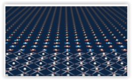
A new study discovers how the sudden excitation of lattice vibrations in a crystal can trigger a change of the magnetic properties of an atomically-thin layer that lies on its surface.
A research team, led by scientists of the Max Planck Institute for the Structure and Dynamics of Matter at CFEL in Hamburg, the University of Oxford, and the Université de Genève, used extremely short X-ray pulses from a free-electron laser to discover that melting of magnetic order in the thin layer is initiated at its interface with the substrate and progressively moves into the interior of the film on an ultra-short time scale. This novel type of ultrafast light control in materials engineered at the atomic scale may lead to new prospects in magnetic storage technologies. The results are reported online in the journal Nature Materials.
Transition metal oxides, such as manganites, cuprates or nickelates, have attracted enormous interest among researchers since their electric and magnetic properties can be altered by even subtle changes of external parameters, such as temperature, and electric or magnetic fields. “But there is also a strong correlation between the atomic arrangement of the crystal lattice and these properties, so that controlled structural modifications allow for tuning the electronic and magnetic state of these materials, too,” said Michael Först, scientist at the Max Planck Institute and one of the lead authors of this work.
More recently, researchers started studying heterostructures composed of different oxide materials. An atomically-thin oxide film on a substrate can have properties very different from its bulk form due to a variety of interface effects, including mechanical strain produced at the interface between the substrate and the film. This makes complex oxide heterostructures a versatile tool for engineering materials and devices properties. “In the present work, we studied the possibility to dynamically control the properties of a thin functional film by modifying the atomic structure of the substrate with light,” said Andrea Caviglia, now at the Kavli Institute of Nanoscience at Delft University of Technology.
At cryogenic temperatures, neodymium nickelate (NdNiO3) is an antiferromagnetic insulator, i.e. the spins of the valence electrons align in an alternating pattern with no resulting net magnetization. Above 200 K, this material becomes a metal and the antiferromagnetic spin ordering disappears concomitantly. When an epitaxial NdNiO3 thin film is grown on a lanthanum aluminate (LaAlO3) substrate, the slightly different lattice constants of the two materials induce static strain in the film leading to a reduction of the insulator–metal-transition temperature from 200 K of the bulk material to about 130 K.
Interestingly, the electrical properties of the NdNiO3 film can be changed on ultrafast time scales by selectively exciting lattice vibrations in the LaAlO3 substrate. This was shown in an earlier publication of the main authors in Physical Review Letters. “In that experiment, a mid-infrared laser pulse at 15 µm wavelength triggered a vibrational mode in the substrate and a drastic change of electrical conductivity in the nickelate film was observed by measuring the change of the sample reflectivity with a terahertz, that is far-infrared, pulse,” said Caviglia.
In the current work, the group studied the effect this substrate excitation has on the magnetic properties of the nickelate film. To measure these changes with high spatial and temporal resolution, the team used a technique called time-resolved resonant soft X-ray diffraction at the Linac Coherent Light Source (LCLS) free-electron laser at SLAC, California. The LCLS femtosecond X-ray pulses scatter off the film, carrying time-stamped signatures of the material’s spin ordering that the physicists then used to reconstruct the spatiotemporal magnetic dynamics.
First, the researchers found that the magnetic ordering melts on a timescale of few picoseconds, i.e. at similar time scales as the insulator–metal transition observed earlier, thus suggesting that both processes are connected.
“Even more interestingly, the diffraction experiment showed that the magnetic melting in the nickelate starts locally at the interface to the substrate and propagates, comparable to a wave, from there into the NdNiO3 film,” said Först. “The high speed at which this wave front propagates, indicates that these dynamics are driven by local changes of the electronic structure at the interface”, he added.
Indeed, a theoretical model, assuming the creation of freely movable charge carriers at the hetero-interface by the substrate lattice vibrations, supports this picture. These charges are likely to scramble the antiferromagnetic order as they propagate into the film.
This work was made possible by the ERC Synergy Grant “Frontiers in Quantum Materials’ Control” (Q-MAC), which brings together scientists from the institutions listed above. Further institutions involved in the collaboration are the Diamond Light Source, the Brookhaven National Laboratory, the Lawrence Berkeley National Laboratory, the Stanford Linear Accelerator Center, and the National University of Singapore. CFEL is a cooperation of DESY, the Max Planck Society and the University of Hamburg.
Share on:


Testimonial
"Our marketing partnership with I-Connect007 is already delivering. Just a day after our press release went live, we received a direct inquiry about our updated products!"
Rachael Temple - AlltematedSuggested Items
Curing and Verification in PCB Shadow Areas
09/17/2025 | Doug Katze, DymaxDesign engineers know a simple truth that often complicates electronics manufacturing: Light doesn’t go around corners. In densely populated PCBs, adhesives and coatings often fail to fully cure in shadowed regions created by tall ICs, connectors, relays, and tight housings.
Marcy’s Musings: Advancing the Advanced Materials Discussion
09/17/2025 | Marcy LaRont -- Column: Marcy's MusingsAs the industry’s most trusted global source of original content about the electronics supply chain, we continually ask you about your concerns, what you care about, and what you most want to learn about. Your responses are insightful and valuable. Thank you for caring enough to provide useful feedback and engage in dialogue.
September 2025 PCB007 Magazine: The Future of Advanced Materials
09/16/2025 | I-Connect007 Editorial TeamMoore’s Law is no more, and the advanced material solutions being developed to grapple with this reality are surprising, stunning, and perhaps a bit daunting. Buckle up for a dive into advanced materials and a glimpse into the next chapters of electronics manufacturing.
I-Connect007 Launches Advanced Electronics Packaging Digest
09/15/2025 | I-Connect007I-Connect007 is pleased to announce the launch of Advanced Electronics Packaging Digest (AEPD), a new monthly digital newsletter dedicated to one of the most critical and rapidly evolving areas of electronics manufacturing: advanced packaging at the interconnect level.
Panasonic Industry will Double the Production Capacity of MEGTRON Multi-layer Circuit Board Materials Over the Next Five Years
09/15/2025 | Panasonic Industry Co., Ltd.Panasonic Industry Co., Ltd., a Panasonic Group company, announced plans for a major expansion of its global production capacity for MEGTRON multi-layer circuit board materials today. The company plans to double its production over the next five years to meet growing demand in the AI server and ICT infrastructure markets.