


 The Marketing Minute: Cracking the Code of Technical Marketing
 Trouble in Your Tank: Implementing Direct Metallization in Advanced Substrate Packaging


New Technique to Synthesise Nanostructured Nanowires
July 17, 2015 | University of CambridgeEstimated reading time: 2 minutes
Researchers have developed a new method for growing ‘hybrid’ crystals at the nanoscale, in which quantum dots – essentially nanoscale semiconductors – of different materials can be sequentially incorporated into a host nanowire with perfect junctions between the components.
A new approach to self-assemble and tailor complex structures at the nanoscale, developed by an international collaboration led by the University of Cambridge and IBM, opens opportunities to tailor properties and functionalities of materials for a wide range of semiconductor device applications.
The researchers have developed a method for growing combinations of different materials in a needle-shaped crystal called a nanowire. Nanowires are small structures, only a few billionths of a metre in diameter. Semiconductors can be grown into nanowires, and the result is a useful building block for electrical, optical, and energy harvesting devices. The researchers have found out how to grow smaller crystals within the nanowire, forming a structure like a crystal rod with an embedded array of gems. Details of the new method are published in the journal Nature Materials.
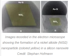
“The key to building functional nanoscale devices is to control materials and their interfaces at the atomic level,” said Dr Stephan Hofmann of the Department of Engineering, one of the paper’s senior authors. “We’ve developed a method of engineering inclusions of different materials so that we can make complex structures in a very precise way.”
Nanowires are often grown through a process called Vapour-Liquid-Solid (VLS) synthesis, where a tiny catalytic droplet is used to seed and feed the nanowire, so that it self-assembles one atomic layer at a time. VLS allows a high degree of control over the resulting nanowire: composition, diameter, growth direction, branching, kinking and crystal structure can be controlled by tuning the self-assembly conditions. As nanowires become better controlled, new applications become possible.
The technique that Hofmann and his colleagues from Cambridge and IBM developed can be thought of as an expansion of the concept that underlies conventional VLS growth. The researchers use the catalytic droplet not only to grow the nanowire, but also to form new materials within it. These tiny crystals form in the liquid, but later attach to the nanowire and then become embedded as the nanowire is grown further. This catalyst mediated docking process can ‘self-optimise’ to create highly perfect interfaces for the embedded crystals.
To unravel the complexities of this process, the research team used two customised electron microscopes, one at IBM’s TJ Watson Research Center and a second at Brookhaven National Laboratory. This allowed them to record high-speed movies of the nanowire growth as it happens atom-by-atom. The researchers found that using the catalyst as a ‘mixing bowl’, with the order and amount of each ingredient programmed into a desired recipe, resulted in complex structures consisting of nanowires with embedded nanoscale crystals, or quantum dots, of controlled size and position.
“The technique allows two different materials to be incorporated into the same nanowire, even if the lattice structures of the two crystals don’t perfectly match,” said Hofmann. “It’s a flexible platform that can be used for different technologies.”
Possible applications for this technique range from atomically perfect buried interconnects to single-electron transistors, high-density memories, light emission, semiconductor lasers, and tunnel diodes, along with the capability to engineer three-dimensional device structures.
“This process has enabled us to understand the behaviour of nanoscale materials in unprecedented detail, and that knowledge can now be applied to other processes,” said Hofmann.
Share on:


Testimonial
"Advertising in PCB007 Magazine has been a great way to showcase our bare board testers to the right audience. The I-Connect007 team makes the process smooth and professional. We’re proud to be featured in such a trusted publication."
Klaus Koziol - atgSuggested Items
Curing and Verification in PCB Shadow Areas
09/17/2025 | Doug Katze, DymaxDesign engineers know a simple truth that often complicates electronics manufacturing: Light doesn’t go around corners. In densely populated PCBs, adhesives and coatings often fail to fully cure in shadowed regions created by tall ICs, connectors, relays, and tight housings.
Marcy’s Musings: Advancing the Advanced Materials Discussion
09/17/2025 | Marcy LaRont -- Column: Marcy's MusingsAs the industry’s most trusted global source of original content about the electronics supply chain, we continually ask you about your concerns, what you care about, and what you most want to learn about. Your responses are insightful and valuable. Thank you for caring enough to provide useful feedback and engage in dialogue.
September 2025 PCB007 Magazine: The Future of Advanced Materials
09/16/2025 | I-Connect007 Editorial TeamMoore’s Law is no more, and the advanced material solutions being developed to grapple with this reality are surprising, stunning, and perhaps a bit daunting. Buckle up for a dive into advanced materials and a glimpse into the next chapters of electronics manufacturing.
I-Connect007 Launches Advanced Electronics Packaging Digest
09/15/2025 | I-Connect007I-Connect007 is pleased to announce the launch of Advanced Electronics Packaging Digest (AEPD), a new monthly digital newsletter dedicated to one of the most critical and rapidly evolving areas of electronics manufacturing: advanced packaging at the interconnect level.
Panasonic Industry will Double the Production Capacity of MEGTRON Multi-layer Circuit Board Materials Over the Next Five Years
09/15/2025 | Panasonic Industry Co., Ltd.Panasonic Industry Co., Ltd., a Panasonic Group company, announced plans for a major expansion of its global production capacity for MEGTRON multi-layer circuit board materials today. The company plans to double its production over the next five years to meet growing demand in the AI server and ICT infrastructure markets.