


 The Marketing Minute: Cracking the Code of Technical Marketing
 Trouble in Your Tank: Implementing Direct Metallization in Advanced Substrate Packaging


Synthesizing Graphene in Silicon Microelectronics
July 22, 2015 | AIP.orgEstimated reading time: 3 minutes
In the last decade, graphene has been intensively studied for its unique optical, mechanical, electrical and structural properties. The one-atom-thick carbon sheets could revolutionize the way electronic devices are manufactured and lead to faster transistors, cheaper solar cells, new types of sensors and more efficient bioelectric sensory devices. As a potential contact electrode and interconnection material, wafer-scale graphene could be an essential component in microelectronic circuits, but most graphene fabrication methods are not compatible with silicon microelectronics, thus blocking graphene's leap from potential wonder material to actual profit-maker.
Now researchers from Korea University, in Seoul, have developed an easy and microelectronics-compatible method to grow graphene and have successfully synthesized wafer-scale (four inches in diameter), high-quality, multi-layer graphene on silicon substrates. The method is based on an ion implantation technique, a process in which ions are accelerated under an electrical field and smashed into a semiconductor. The impacting ions change the physical, chemical or electrical properties of the semiconductor.
In a paper published this week in the journal Applied Physics Letters, from AIP Publishing, the researchers describe their work, which takes graphene a step closer to commercial applications in silicon microelectronics.
"For integrating graphene into advanced silicon microelectronics, large-area graphene free of wrinkles, tears and residues must be deposited on silicon wafers at low temperatures, which cannot be achieved with conventional graphene synthesis techniques as they often require high temperatures," said Jihyun Kim, the team leader and a professor in the Department of Chemical and Biological Engineering at Korea University. "Our work shows that the carbon ion implantation technique has great potential for the direct synthesis of wafer-scale graphene for integrated circuit technologies."
Discovered just over a decade ago, graphene is now considered the thinnest, lightest and strongest material in the world. Graphene is completely flexible and transparent while being inexpensive and non-toxic, and it can conduct electricity as well as copper, carrying electrons with almost no resistance even at room temperature, a property known as ballistic transport. Graphene's unique optical, mechanical and electrical properties have lead to the one-atom-thick form of carbon being heralded as the next generation material for faster, smaller, cheaper and less power-hungry electronics.
"In silicon microelectronics, graphene is a potential contact electrode and an interconnection material linking semiconductor devices to form the desired electrical circuits," said Kim. "This renders high processing temperature undesirable, as temperature-induced damage, strains, metal spiking and unintentional diffusion of dopants may occur."
Thus, although the conventional graphene fabrication method of chemical vapor deposition is widely used for the large-area synthesis of graphene on copper and nickel films, the method is not suited for silicon microelectronics, as chemical vapor deposition would require a high growth temperature above 1,000 degrees Celsius and a subsequent transfer process of the graphene from the metallic film to the silicon.
"The transferred graphene on the target substrate often contains cracks, wrinkles and contaminants," said Kim. "Thus, we are motivated to develop a transfer-free method to directly synthesize high quality, multilayer graphene in silicon microelectronics."
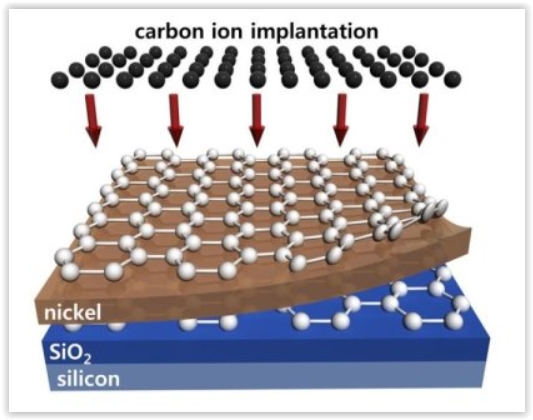
Kim's method relies on ion implantation, a microelectronics-compatible technique normally used to introduce impurities into semiconductors. In the process, carbon ions were accelerated under an electrical field and bombarded onto a layered surface made of nickel, silicon dioxide and silicon at the temperature of 500 degrees Celsius. The nickel layer, with high carbon solubility, is used as a catalyst for graphene synthesis. The process is then followed by high temperature activation annealing (about 600 to 900 degrees Celsius) to form a honeycomb lattice of carbon atoms, a typical microscopic structure of graphene.
CREDIT: J.Kim/Korea University, Korea" height="639" width="820">
Wafer-scale (4 inch in diameter) synthesis of multi-layer graphene using high-temperature carbon ion implantation on nickel / SiO2 /silicon.
CREDIT: J.Kim/Korea University, Korea
Kim explained that the activation annealing temperature could be lowered by performing the ion implantation at an elevated temperature. Kim and his colleagues then systematically studied the effects of the annealing conditions on the synthesis of high-quality, multi-layer graphene by varying the ambient pressure, ambient gas, temperature and time during the treatment.
According to Kim, the ion implantation technique also offers finer control on the final structure of the product than other fabrication methods, as the graphene layer thickness can be precisely determined by controlling the dose of carbon ion implantation.
"Our synthesis method is controllable and scalable, allowing us to obtain graphene as large as the size of the silicon wafer [over 300 millimeters in diameter]," Kim said.
The researchers' next step is to further lower the temperature in the synthesis process and to control the thickness of the graphene for manufacturing production.
Share on:


Testimonial
"We’re proud to call I-Connect007 a trusted partner. Their innovative approach and industry insight made our podcast collaboration a success by connecting us with the right audience and delivering real results."
Julia McCaffrey - NCAB GroupSuggested Items
Trouble in Your Tank: Implementing Direct Metallization in Advanced Substrate Packaging
09/15/2025 | Michael Carano -- Column: Trouble in Your TankDirect metallization systems based on conductive graphite are gaining popularity throughout the world. The environmental and productivity gains achievable with this process are outstanding. Direct metallization reduces the costs of compliance, waste treatment, and legal issues related to chemical exposure. A graphite-based direct plate system has been devised to address these needs.
Closing the Loop on PCB Etching Waste
09/09/2025 | Shawn Stone, IECAs the PCB industry continues its push toward greener, more cost-efficient operations, Sigma Engineering’s Mecer System offers a comprehensive solution to two of the industry’s most persistent pain points: etchant consumption and rinse water waste. Designed as a modular, fully automated platform, the Mecer System regenerates spent copper etchants—both alkaline and acidic—and simultaneously recycles rinse water, transforming a traditionally linear chemical process into a closed-loop system.
Driving Innovation: Depth Routing Processes—Achieving Unparalleled Precision in Complex PCBs
09/08/2025 | Kurt Palmer -- Column: Driving InnovationIn PCB manufacturing, the demand for increasingly complex and miniaturized designs continually pushes the boundaries of traditional fabrication methods, including depth routing. Success in these applications demands not only on robust machinery but also sophisticated control functions. PCB manufacturers rely on advanced machine features and process methodologies to meet their precise depth routing goals. Here, I’ll explore some crucial functions that empower manufacturers to master complex depth routing challenges.
Trouble in Your Tank: Minimizing Small-via Defects for High-reliability PCBs
08/27/2025 | Michael Carano -- Column: Trouble in Your TankTo quote the comedian Stephen Wright, “If at first you don’t succeed, then skydiving is not for you.” That can be the battle cry when you find that only small-diameter vias are exhibiting voids. Why are small holes more prone to voids than larger vias when processed through electroless copper? There are several reasons.
The Government Circuit: Navigating New Trade Headwinds and New Partnerships
08/25/2025 | Chris Mitchell -- Column: The Government CircuitAs global trade winds continue to howl, the electronics manufacturing industry finds itself at a critical juncture. After months of warnings, the U.S. Government has implemented a broad array of tariff increases, with fresh duties hitting copper-based products, semiconductors, and imports from many nations. On the positive side, tentative trade agreements with Europe, China, Japan, and other nations are providing at least some clarity and counterbalance.