


 The Marketing Minute: Cracking the Code of Technical Marketing
 Trouble in Your Tank: Implementing Direct Metallization in Advanced Substrate Packaging


NIST Shows Organic Solar Industry Something New Under the Sun
July 23, 2015 | NISTEstimated reading time: 2 minutes
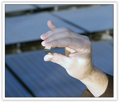
Hunting for the best material from which to build organic solar cells can be like seeking the proverbial haystack needle, but now scientists at the National Institute of Standards and Technology (NIST) and the Naval Research Laboratory may have a better search tool for the nascent industry.
The team's research findings in Nature Communications* show it is possible to test a candidate material quickly and directly, using off-the-shelf laser technology. The method bypasses the costly, time-consuming step of constructing a prototype solar cell for each material to be evaluated.
"We'd like to give companies and manufacturers an alternative to trial and error," says NIST research chemist Ted Heilweil. "It takes a long time to develop photovoltaic materials for market. Screening them using our method would be much faster."
Organic materials (e.g. plastics) hold a particular attraction for the solar industry, largely because of their comparative low cost and physical flexibility. Organics inspire the possibility of one day painting an inexpensive solar array onto most any surface, even one that bends and moves, and simply replacing it with a fresh coat when it wears out.
At this point, organics are far less efficient at converting sunlight to electricity than traditional silicon-based technology, but ideas for better materials come at a fast clip. Unfortunately, sifting through these candidates and zeroing in on the most promising ones is expensive and arduous. Because it entails building a prototype cell for each prospective material, relatively few candidates get tested.
The team's new method sidesteps this problem by using ultrafast lasers to probe a candidate material's abilities directly—and without electrical contacts. They found that when shining pulses of visible light onto a sample to mimic the sun, they could probe the sample's electronic behavior with a second laser pulse near the microwave range of the spectrum. When the sample absorbs these "terahertz" waves, its properties change in easily detectable ways. Just how the terahertz pulse changes is dependent on the material's viability at converting light to electricity.
To test their method, the team looked at a number of mixed organic molecules and polymers whose abilities were well-understood from conventional prototyping.
"We looked at small organics and polymers that people in the solar industry have been using as benchmarks, and we saw the same relative behavior with our terahertz measurements," Heilweil says. "We're pretty confident that our method can tell you what is useful to know."
The team is using the method as part of its own ongoing materials search, Heilweil says.
Share on:


Testimonial
"We’re proud to call I-Connect007 a trusted partner. Their innovative approach and industry insight made our podcast collaboration a success by connecting us with the right audience and delivering real results."
Julia McCaffrey - NCAB GroupSuggested Items
Curing and Verification in PCB Shadow Areas
09/17/2025 | Doug Katze, DymaxDesign engineers know a simple truth that often complicates electronics manufacturing: Light doesn’t go around corners. In densely populated PCBs, adhesives and coatings often fail to fully cure in shadowed regions created by tall ICs, connectors, relays, and tight housings.
Marcy’s Musings: Advancing the Advanced Materials Discussion
09/17/2025 | Marcy LaRont -- Column: Marcy's MusingsAs the industry’s most trusted global source of original content about the electronics supply chain, we continually ask you about your concerns, what you care about, and what you most want to learn about. Your responses are insightful and valuable. Thank you for caring enough to provide useful feedback and engage in dialogue.
September 2025 PCB007 Magazine: The Future of Advanced Materials
09/16/2025 | I-Connect007 Editorial TeamMoore’s Law is no more, and the advanced material solutions being developed to grapple with this reality are surprising, stunning, and perhaps a bit daunting. Buckle up for a dive into advanced materials and a glimpse into the next chapters of electronics manufacturing.
I-Connect007 Launches Advanced Electronics Packaging Digest
09/15/2025 | I-Connect007I-Connect007 is pleased to announce the launch of Advanced Electronics Packaging Digest (AEPD), a new monthly digital newsletter dedicated to one of the most critical and rapidly evolving areas of electronics manufacturing: advanced packaging at the interconnect level.
Panasonic Industry will Double the Production Capacity of MEGTRON Multi-layer Circuit Board Materials Over the Next Five Years
09/15/2025 | Panasonic Industry Co., Ltd.Panasonic Industry Co., Ltd., a Panasonic Group company, announced plans for a major expansion of its global production capacity for MEGTRON multi-layer circuit board materials today. The company plans to double its production over the next five years to meet growing demand in the AI server and ICT infrastructure markets.