


 Dan’s Biz Bookshelf: Four Important Books You Need to Read (Not Just Say You Have)
 The Marketing Minute: Cracking the Code of Technical Marketing


Magnetic Material Unnecessary to Create Spin Current
July 28, 2015 | Argonne National LaboratoryEstimated reading time: 3 minutes
It doesn’t happen often that a young scientist makes a significant and unexpected discovery, but postdoctoral researcher Stephen Wu of the U.S. Department of Energy's Argonne National Laboratory just did exactly that. What he found—that you don't need a magnetic material to create spin current from insulators—has important implications for the field of spintronics and the development of high-speed, low-power electronics that use electron spin rather than charge to carry information.
Wu’s work upends prevailing ideas of how to generate a current of spins. “This is a discovery in the true sense,” said Anand Bhattacharya, a physicist in Argonne's Materials Science Division and the Center for Nanoscale Materials (a DOE Office of Science user facility), who is the project's principal investigator. “There’s no prediction of anything like it.”
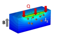
Spin is a quantum property of electrons that scientists often compare to a tiny bar magnet that points either “up” or “down.” Until now scientists and engineers have relied on shrinking electronics to make them faster, but now increasingly clever methods must be used to sustain the continued progression of electronics technology, as we reach the limit of how small we can create a transistor. One such method is to separate the flow of electron spin from the flow of electron current, upending the idea that information needs to be carried on wires and instead flowing it through insulators.
To create a current of spins in insulators, scientists have typically kept electrons stationary in a lattice made of an insulating ferromagnetic material, such as yttrium iron garnet (YIG). When they apply a heat gradient across the material, the spins begin to “move”—that is, information about the orientation of a spin is communicated from one point to another along the lattice, much in the way a wave moves through water without actually transporting the water molecules anywhere. Spin excitations known as magnons are thought to carry the current.
Wu set out to build on previous work with spin currents, expanding it to different materials using a new technique he’d developed. He worked on making devices a thousand times smaller than the typical systems used, giving him more control over the heat and allowing him to create larger thermal gradients in a smaller area. “That was the key to why we were able to do this experiment,” he says.
Wu looked at a layer of ferromagnetic YIG on a substrate of paramagnetic gadolinium gallium garnet (GGG). He expected to see no action from the GGG: in a paramagnet the spins aren’t aligned as they are in a ferromagnet. They generate no magnetic field, produce no magnons, and there appears to be no way for the spins to communicate with one another. But to everyone’s surprise, the spin current was stronger in the GGG than it was in the YIG. “The spins in the system were not talking to each other. But we still found measurable spin current,” says Wu. “This effect shouldn’t happen at all.”
The next step is to figure out why it does.
“We don’t know the way this works,” said Bhattacharya. “There’s an opportunity here for somebody to come up with a theory for this.”
The scientists also want to look for other materials that display this effect. “We think that there may be other new physics working here,” said Bhattacharya. “Because, since the material is not a ferromagnet, the objects that are moving the spin are not what we typically understand.”
In the meantime, said Wu, “We’ve just taken ferromagnetism off its pedestal. In a spintronic device you don’t have to use a ferromagnet. You can use either a paramagnetic metal or a paramagnetic insulator to do it now.”
For more information, see the paper, "Paramagnetic spin Seebeck effect," published in the journal Physical Review Letters.
This work was supported by the DOE Office of Science. The Center for Nanoscale Materials is a DOE Office of Science User Facility.
Argonne National Laboratory seeks solutions to pressing national problems in science and technology. The nation's first national laboratory, Argonne conducts leading-edge basic and applied scientific research in virtually every scientific discipline. Argonne researchers work closely with researchers from hundreds of companies, universities, and federal, state and municipal agencies to help them solve their specific problems, advance America's scientific leadership and prepare the nation for a better future. With employees from more than 60 nations, Argonne is managed by UChicago Argonne, LLC for the U.S. Department of Energy's Office of Science.
The Office of Science is the single largest supporter of basic research in the physical sciences in the United States, and is working to address some of the most pressing challenges of our time. For more information, please visit science.energy.gov.
Share on:


Testimonial
"We’re proud to call I-Connect007 a trusted partner. Their innovative approach and industry insight made our podcast collaboration a success by connecting us with the right audience and delivering real results."
Julia McCaffrey - NCAB GroupSuggested Items
Curing and Verification in PCB Shadow Areas
09/17/2025 | Doug Katze, DymaxDesign engineers know a simple truth that often complicates electronics manufacturing: Light doesn’t go around corners. In densely populated PCBs, adhesives and coatings often fail to fully cure in shadowed regions created by tall ICs, connectors, relays, and tight housings.
Marcy’s Musings: Advancing the Advanced Materials Discussion
09/17/2025 | Marcy LaRont -- Column: Marcy's MusingsAs the industry’s most trusted global source of original content about the electronics supply chain, we continually ask you about your concerns, what you care about, and what you most want to learn about. Your responses are insightful and valuable. Thank you for caring enough to provide useful feedback and engage in dialogue.
September 2025 PCB007 Magazine: The Future of Advanced Materials
09/16/2025 | I-Connect007 Editorial TeamMoore’s Law is no more, and the advanced material solutions being developed to grapple with this reality are surprising, stunning, and perhaps a bit daunting. Buckle up for a dive into advanced materials and a glimpse into the next chapters of electronics manufacturing.
I-Connect007 Launches Advanced Electronics Packaging Digest
09/15/2025 | I-Connect007I-Connect007 is pleased to announce the launch of Advanced Electronics Packaging Digest (AEPD), a new monthly digital newsletter dedicated to one of the most critical and rapidly evolving areas of electronics manufacturing: advanced packaging at the interconnect level.
Panasonic Industry will Double the Production Capacity of MEGTRON Multi-layer Circuit Board Materials Over the Next Five Years
09/15/2025 | Panasonic Industry Co., Ltd.Panasonic Industry Co., Ltd., a Panasonic Group company, announced plans for a major expansion of its global production capacity for MEGTRON multi-layer circuit board materials today. The company plans to double its production over the next five years to meet growing demand in the AI server and ICT infrastructure markets.