


 Dan’s Biz Bookshelf: Four Important Books You Need to Read (Not Just Say You Have)
 The Marketing Minute: Cracking the Code of Technical Marketing


Battery Buffer Takes the Strain
July 30, 2015 | CASEstimated reading time: 1 minute
Researchers in China and the US have developed a layered oxide that shrinks when ions are intercalated into it, with the hope of buffering the volume expansion seen in common electrode materials.
Layered oxide materials are very stable, contain large interstitial spaces, and often undergo a volume change, or “strain effect”, when ions are incorporated into their structure. This volume change is detrimental to the electrode as it often results in inferior long-term cycling stability and reduced battery safety. So-called zero-strain materials, where no volume change is seen, are ideal electrode materials. However, these are very rare and most layered oxides exhibit a positive strain effect.
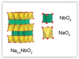
Many layered oxides have the formula AxMO2, and consist of stacked (MO2)n sheets with edge-sharing MO6 octahedra, in between which alkali metal atoms are located at octahedral, tetrahedral, and prismatic sites. Now, Xuefeng Wang at the Chinese Academy of Sciences and co-workers have synthesised Na0.5NbO2, a layered oxide in which the NbO6 clusters are edge-sharing trigonal prisms rather than octahedra. In this structure the sodium and niobium ions are positioned contrary to conventional layered materials.
Na0.5NbO2 is a rare negative-strain material with high stability, a long cycling life and an impressive rate performance. As Jang Wook Choi, a researcher in the Energy Nanomaterials Group at the Korea Advanced Institute of Science and Technology explains, ‘this is opposite to other cases or common sense, as the volume shrinks even after you put something inside the structure.’ The negative volume effect appears to be a result of enhanced interlayer Na–O interactions and weakened Nb–Nb and Nb–O bonding on sodium intercalation.
Wang and colleagues evaluated Na0.5NbO2 both as an independent electrode material, and as a buffer in composite electrodes with positive-strain materials, in which it counteracts the volume expansion caused by a positive strain effect. The material had a more significant volume effect than other volume buffer materials, as well as being electrically conductive and compatible with electrolytes at the required voltage.
'The limitation of our system lies in the high cost of niobium and the difficulty of synthesis,’ says Wang. ‘But we think that these results will influence the thinking about layered structures and how to design a better electrode for rechargeable batteries.’ (Royal Society of Chemistry)
Share on:


Testimonial
"Advertising in PCB007 Magazine has been a great way to showcase our bare board testers to the right audience. The I-Connect007 team makes the process smooth and professional. We’re proud to be featured in such a trusted publication."
Klaus Koziol - atgSuggested Items
Curing and Verification in PCB Shadow Areas
09/17/2025 | Doug Katze, DymaxDesign engineers know a simple truth that often complicates electronics manufacturing: Light doesn’t go around corners. In densely populated PCBs, adhesives and coatings often fail to fully cure in shadowed regions created by tall ICs, connectors, relays, and tight housings.
Marcy’s Musings: Advancing the Advanced Materials Discussion
09/17/2025 | Marcy LaRont -- Column: Marcy's MusingsAs the industry’s most trusted global source of original content about the electronics supply chain, we continually ask you about your concerns, what you care about, and what you most want to learn about. Your responses are insightful and valuable. Thank you for caring enough to provide useful feedback and engage in dialogue.
September 2025 PCB007 Magazine: The Future of Advanced Materials
09/16/2025 | I-Connect007 Editorial TeamMoore’s Law is no more, and the advanced material solutions being developed to grapple with this reality are surprising, stunning, and perhaps a bit daunting. Buckle up for a dive into advanced materials and a glimpse into the next chapters of electronics manufacturing.
I-Connect007 Launches Advanced Electronics Packaging Digest
09/15/2025 | I-Connect007I-Connect007 is pleased to announce the launch of Advanced Electronics Packaging Digest (AEPD), a new monthly digital newsletter dedicated to one of the most critical and rapidly evolving areas of electronics manufacturing: advanced packaging at the interconnect level.
Panasonic Industry will Double the Production Capacity of MEGTRON Multi-layer Circuit Board Materials Over the Next Five Years
09/15/2025 | Panasonic Industry Co., Ltd.Panasonic Industry Co., Ltd., a Panasonic Group company, announced plans for a major expansion of its global production capacity for MEGTRON multi-layer circuit board materials today. The company plans to double its production over the next five years to meet growing demand in the AI server and ICT infrastructure markets.