


 Dan’s Biz Bookshelf: Four Important Books You Need to Read (Not Just Say You Have)
 The Marketing Minute: Cracking the Code of Technical Marketing


Scientists Curve Nanoparticle Sheets into Complex Forms
August 3, 2015 | Argonne National LaboratoryEstimated reading time: 4 minutes
Scientists have been making nanoparticles for more than two decades in two-dimensional sheets, three-dimensional crystals and random clusters. But they have never been able to get a sheet of nanoparticles to curve or fold into a complex three-dimensional structure. Now researchers from the University of Chicago, the University of Missouri and the U.S. Department of Energy's Argonne National Laboratory have found a simple way to do exactly that.
The findings open the way for scientists to design membranes with tunable electrical, magnetic and mechanical properties that could be used in electronics and may even have implications for understanding biological systems.
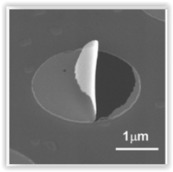
Argonne researchers are able to fold gold nanoparticle membranes in a specific direction using an electron beam because two sides of the membrane are different. Image credit: Xiao-Min Lin et. al, taken at Argonne’s Electron Microscopy Center.
Working at the Center for Nanoscale Materials (CNM) and the Advanced Photon Source (APS), two DOE Office of Science User Facilities located at Argonne, the team got membranes of gold nanoparticles coated with organic molecules to curl into tubes when hit with an electron beam. Equally importantly, they have discovered how and why it happens.
The scientists coat gold nanoparticles of a few thousand atoms each with an oil-like organic molecule that holds the gold particles together. When floated on water the particles form a sheet; when the water evaporates, it leaves the sheet suspended over a hole. “It’s almost like a drumhead,” says Xiao-Min Lin, the staff scientist at the Center for Nanoscale Materials who led the project. “But it’s a very thin membrane made of a single layer of nanoparticles.”
To their surprise, when the scientists put the membrane into the beam of a scanning electron microscope, it folded. It folded every time, and always in the same direction.
“That got our curiosity up,” said Lin. “Why is it bending in one direction?”
The answer lay in the organic surface molecules. They are hydrophobic: when floated on water they try to avoid contact with it, so they end up distributing themselves in a non-uniform way across the top and bottom layers of the nanoparticle sheet. When the electron beam hits the molecules on the surface it causes them to form an additional bond with their neighbors, creating an asymmetrical stress that makes the membranes fold.
Zhang Jiang and Jin Wang, X-ray staff at the APS, came up with an ingenious way to measure the molecular asymmetry, which at only six angstroms, or about six atoms thick, is so tiny it would not normally be measurable.
Subramanian Sankaranarayanan and Sanket Deshmukh at CNM used the high-performance computing resources at DOE’s National Energy Research Scientific Computing Center and the Argonne Leadership Computing Facility (ALCF), both DOE Office of Science User Facilities, to analyze the surface of the nanoparticles. They discovered that the amount of surface covered by the organic molecules and the molecules’ mobility on the surface both have an important influence on the degree of asymmetry in the membrane.
“These are fascinating results,” said Fernando Bresme, professor of chemical physics at the Imperial College in London and a leading theorist on soft matter physics. “They advance significantly our ability to make new nano-structures with controlled shapes.”
In principle, scientists could use this method to induce folding in any nanoparticle membrane that has an asymmetrical distribution of surface molecules. Said Lin, “You use one type of molecule that hates water and rely on the water surfaces to drive the molecules to distribute non-uniformly, or you could use two different kinds of molecules. The key is that the molecules have to distribute non-uniformly.”
The next step for Lin and his colleagues is to explore how they can control the molecular distribution on the surface and therefore the folding behavior. They envision zapping only a small part of the structure with the electron beam, designing the stresses to achieve particular bending patterns.
“You can maybe fold these things into origami structures and all sorts of interesting geometries,” Lin said. “It opens the possibilities.”
About Argonne National Laboratory
Argonne National Laboratory seeks solutions to pressing national problems in science and technology. The nation's first national laboratory, Argonne conducts leading-edge basic and applied scientific research in virtually every scientific discipline. Argonne researchers work closely with researchers from hundreds of companies, universities, and federal, state and municipal agencies to help them solve their specific problems, advance America's scientific leadership and prepare the nation for a better future. With employees from more than 60 nations, Argonne is managed by UChicago Argonne, LLC for the U.S. Department of Energy's Office of Science. For more, www.anl.gov.
About DOE’s Office of Science
DOE’s Office of Science is the single largest supporter of basic research in the physical sciences in the United States, and is working to address some of the most pressing challenges of our time. For more information, please visit science.energy.gov.
Share on:


Testimonial
"The I-Connect007 team is outstanding—kind, responsive, and a true marketing partner. Their design team created fresh, eye-catching ads, and their editorial support polished our content to let our brand shine. Thank you all! "
Sweeney Ng - CEE PCBSuggested Items
Driving Innovation: Depth Routing Processes—Achieving Unparalleled Precision in Complex PCBs
09/08/2025 | Kurt Palmer -- Column: Driving InnovationIn PCB manufacturing, the demand for increasingly complex and miniaturized designs continually pushes the boundaries of traditional fabrication methods, including depth routing. Success in these applications demands not only on robust machinery but also sophisticated control functions. PCB manufacturers rely on advanced machine features and process methodologies to meet their precise depth routing goals. Here, I’ll explore some crucial functions that empower manufacturers to master complex depth routing challenges.
Polar Instruments Announces Additive Transmission Line Support for Si9000e
08/20/2025 | Polar InstrumentsTransmission lines embedded into the PCB surface are a feature of UHDI constructions. The 2025 fall release of Polar's Si9000e PCB impedance & insertion loss transmission line field solver incorporates eight new single ended, differential and coplanar transmission line structures.
Henniker Plasma Launches Stratus Turnkey Plasma Manufacturing Cell
08/13/2025 | Henniker PlasmaHenniker Plasma, a leading manufacturer of plasma treatment systems, proudly announces the launch of its Stratus Plasma Manufacturing Cell range — a fully integrated, turnkey solution that combines advanced atmospheric plasma surface treatment with robotic automation.
Trouble in Your Tank: Metallizing Flexible Circuit Materials—Mitigating Deposit Stress
08/04/2025 | Michael Carano -- Column: Trouble in Your TankMetallizing materials, such as polyimide used for flexible circuitry and high-reliability multilayer printed wiring boards, provide a significant challenge for process engineers. Conventional electroless copper systems often require pre-treatments with hazardous chemicals or have a small process window to achieve uniform coverage without blistering. It all boils down to enhancing the adhesion of the thin film of electroless copper to these smooth surfaces.
Designers Notebook: Basic PCB Planning Criteria—Establishing Design Constraints
07/22/2025 | Vern Solberg -- Column: Designer's NotebookPrinted circuit board development flows more smoothly when all critical issues are predefined and understood from the start. As a basic planning strategy, the designer must first consider the product performance criteria, then determine the specific industry standards or specifications that the product must meet. Planning also includes a review of all significant issues that may affect the product’s manufacture, performance, reliability, overall quality, and safety.