


 Flexible Thinking: Designing Flex Circuits for Dynamic Reliability
 Global PCB Connections: Rigid-flex and Flexible PCBs—The Backbone of Modern Electronics
 Happy’s Tech Talk #29: Bend-to-Install Semi-flex FR-4


Transition from Three to Two Dimensions Increases Conduction
August 5, 2015 | MIPTEstimated reading time: 2 minutes
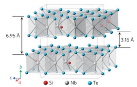
Scientists from the MIPT Department of Molecular and Chemical Physics have for the first time described the behavior of electrons in a previously unstudied analogue of graphene, two-dimensional niobium telluride, and, in the process, uncovered the nature of two-dimensionality effects on conducting properties. These findings will help in the creation of future flat and flexible electronic devices.
In recent decades, physicists have been actively studying so-called two-dimensional materials. Andrei Geim and Konstantin Novoselov received the Nobel Prize for their research on graphene, the most well-known among them. The properties of such materials, which can be described as “sheets” with a thickness of a few atoms, strongly differ from their three-dimensional analogues. For example, graphene is transparent, conducts current better than copper and has good thermal conductivity. Scientists believe that other types of two-dimensional materials may possess even more exotic properties.
A group of scientists from Russia and the USA, including Pavel Sorokin and Liubov Antipina from MIPT, recently conducted research on the properties of the crystals of one such material,Nb3SiTe6, a compound of niobium telluride. In their structure, the crystals resemble sandwiches with a thickness of three atoms (around 4 angstroms): a layer of tellurium, a layer of niobium mixed with silicon atoms and then another layer of tellurium. This substance belongs to a class of materials known as dichalcogenides, which many scientists view as promising two-dimensional semiconductors.
The scientists synthesized Nb3SiTe6 crystals in a laboratory at Tulane University (New Orleans). They then separated them into two-dimensional layers, taking samples for further analysis by transmission electron microscopy, X-ray crystal analysis and other methods. The goal of the researchers was to investigate electron-phonon interaction changes in two-dimensional substances.
Quasi particles, quanta of crystal lattice oscillations, are called phonons. Physicists introduced the concept of phonons because it helped simplify the description of processes in crystals, and tracking of electron-phonon interaction is fundamentally important for description of the different conducting properties in matter.
"We developed a theory that predicts that electron-phonon interaction is suppressed due to dimensional effects in two-dimensional material. In other words, these materials obstruct the flow of electrons to a lesser extent," says Pavel Sorokin, a co-author of the study, doctor of physical and mathematical sciences, and lecturer at the MIPT Section of the Physics and Chemistry of Nanostructures (DMCP).
American colleagues confirmed this predictioninrelatedexperiments. "They conducted measurements where the same effectwas observed. Our calculations allowed the ruling out of other explanations; we managed to prove that changes in electron-phonon interaction occur specifically because of the two-dimensionality of the membrane," Sorokin adds.
Share on:


Testimonial
"Your magazines are a great platform for people to exchange knowledge. Thank you for the work that you do."
Simon Khesin - Schmoll MaschinenSuggested Items
Driving Innovation: Selecting the Right Laser Source
04/28/2026 | Simon Khesin -- Column: Driving InnovationWhen I first joined Schmoll Maschinen, I brought experience from almost every PCB process, except for laser. As I immersed myself in laser processing, I realized why it can seem so daunting to a newcomer. The complexity arises from three intersecting factors: A vast variety of laser sources: CO2, UV-nano, green-pico, UV-pico, IR-pico, and others; a diverse range of applications: Drilling, cutting, ablation, and more; and an extensive list of materials: These have vastly different absorption rates. Choosing the right machine or laser source is rarely trivial. Even for experienced engineers, answering "Which source is best?" requires examining the business's specific goals.
Institute of Circuit Technology Spring Seminar 2026: A Bright Future in Europe
04/23/2026 | Pete Starkey, I-Connect007Through the leafy lanes and spring flowers of Warwickshire and back to Meridan, the traditional centre of England, and now officially part of the Metropolitan Borough of Solihull in the county of the West Midlands, I attended the Annual General Meeting and Spring Seminar of the Institute of Circuit Technology (ICT) on April 14. Out of the AGM came notable changes in leadership at the top of the Institute: the retirement of Mat Beadel as chair and Emma Hudson as technical director. Effective May 1, Steve Driver is the new chair, and Alun Morgan is the new technical director.
ACCM Unveils Negative and Near-zero CTE Materials for Large-Format AI Chips
04/21/2026 | Advanced Chip and Circuit MaterialsAdvanced Chip and Circuit Materials, Inc. (ACCM) has launched two new materials: Celeritas HM50, with a negative coefficient of thermal expansion (CTE) of -8 ppm/°C to offset the positive CTE and expansion of copper with temperature on circuit boards, and Celeritas HM001, with near-zero CTE and the low-loss performance needed for high-speed signal layers to 224 Gb/s and faster in artificial intelligence (AI) circuits.
Fresh PCB Concepts: Designing PCBs for Harsh Environments—Reliability Is Engineered Upstream
04/23/2026 | Team NCAB -- Column: Fresh PCB ConceptsWhen engineers hear the phrase “harsh environment,” they usually think of the extreme temperature swings, vibration and shock, pressure changes, or radiation in aerospace. However, aerospace is not the only harsh environment where electronic assemblies must survive. Automotive power electronics, downhole oil and gas tools, marine controls, rail systems, defense platforms, and industrial automation equipment all expose PCBs to environments that are equally unforgiving. The stress mechanisms may differ, but the physics does not.
Advanced Packaging for AI: Reliability Starts at the Cu/Cu/Cu Microvia Junction
04/20/2026 | Kuldip Johal, MKS' AtotechThe rapid growth of AI computing, from training clusters to inference at scale, is reshaping demand across the entire electronics supply chain. Advances in technology requirements, such as higher bandwidth, lower latency, and greater compute density, are driving the development of advanced packaging technologies and transforming the PCB industry across design, manufacturing, testing, and even architecture.