


 American Made Advocacy: PCBs in the National Spotlight
 Defense Speak Interpreted: Extreme Financial Disparity in Drones and Missiles
 The Right Approach: The End of an Era—DoD Proposes MIL-PRF-31032 Cancellation


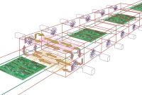
A reflow oven is simply any device that can liquefy solder in a controlled way to produce an electrical conductive bond between the component and its host (the board). There are several different methods to do this, not all of which can literally be called ovens. For instance, the simplest form of heating is performed by conduction, that is, by contact with a heated surface such as a hot plate. Other heating methods typically performed within a chamber (oven) but that rely on different heating methods include:
- Convection: Boards with their assembled components are passed through heated, circulating air from a conventional electrical heat source.
- Infrared (IR): Boards are passed inside a chamber over a direct IR heat source.
- Vapor Phase: Vapor is generated by heating a fluid with a specific boiling point (240°C) and transfers heat to the circuit board just above the melting point of the solder.
Let's begin with a commonly asked question: What size oven do I need? The answer is also a question: How many zones can you afford?
It seems like an odd way to start a discussion about reflow ovens, but it's not entirely unreasonable. As with any complex process, there will be tradeoffs between cost and capabilities, and more zones will always give you better flexibility and more control over your profile—but at a cost. The decision has to be qualified primarily on your anticipated throughput; that is, how many boards you process in a day or a week.
There are other considerations too, such as board size, component density, and appropriate thermal technology, but we’ll talk about those (and more) after identifying the work-flow volume.
A typical soldering operation in today's world requires three main stages for temperature profiling: preheat, soak (activate), and reflow, which perform these functions: 1) The preheat stage for a certain period of time to activation temperature; 2) the soak stage for a different period of time to activate the solder; and 3) the reflow stage where temperatures peak for yet a different time frame. After this, the board is typically cooled and removed. Depending on the material, e.g., leaded, lead-free or specialty materials such as epoxies, the heating profile for each stage will vary according to the manufacturer’s specifications to achieve optimal bonding.
Editor's Note: This article originally appeared in the August 2015 issue of SMT Magazine.


