


 Dan’s Biz Bookshelf: Four Important Books You Need to Read (Not Just Say You Have)
 The Marketing Minute: Cracking the Code of Technical Marketing


"Sandwiching" Atomic Layers Expands Possibilities For Making Materials That Store Energy
August 17, 2015 | Drexel UniversityEstimated reading time: 5 minutes
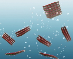
The scientists whose job it is to test the limits of what nature—specifically chemistry— will allow to exist, just set up shop on some new real estate on the Periodic Table. Using a method they invented for joining disparate elemental layers into a stable material with uniform, predictable properties, Drexel University researchers are testing an array of new combinations that may vastly expand the options available to create faster, smaller, more efficient energy storage, advanced electronics and wear-resistant materials.
Led by postdoctoral researcher Babak Anasori, PhD, a team from Drexel’s Department of Materials Science and Engineering created the material-making method, that can sandwich 2-D sheets of elements that otherwise couldn’t be combined in a stable way. And they proved its effectiveness by creating two entirely new, layered two-dimensional materials using molybdenum, titanium and carbon.
“By ‘sandwiching’ one or two atomic layers of a transition metal like titanium, between monoatomic layers of another metal, such as molybdenum, with carbon atoms holding them together, we discovered that a stable material can be produced,” Anasori said. “It was impossible to produce a 2-D material having just three or four molybdenum layers in such structures, but because we added the extra layer of titanium as a connector, we were able to synthesize them.”
The discovery, which was recently published in the journal ACS Nano, is significant because it represents a new way of combining elemental materials to form the building blocks of energy storage technology—such as batteries, capacitors and supercapacitors, as well as superstrong composites—like the ones used in phone cases and body armor. Each new combination of atom-thick layers presents new properties and researchers suspect that one, or more, of these new materials will exhibit energy storage and durability properties so disproportional to its size that it could revolutionize technology in the future.
“While it’s hard to say, at this point, exactly what will become of these new families of 2-D materials we’ve discovered, it is safe to say that this discovery enables the field of materials science and nanotechnology to move into an uncharted territory,” Anasori said.
Mastering Materials
Combining two-dimensional sheets of elements in an organized way to produce new materials has been the goal of Drexel nanomaterials researchers for more than a decade. Imposing this sort of organization at the atomic level is no easy task.
“Due to their structure and electric charge, certain elements just don’t ‘like’ to be combined,” Anasori said. “It’s like trying to stack magnets with the poles facing the same direction—you’re not going to be very successful and you’re going to be picking up a lot of flying magnets.”
But Drexel researchers came up with a clever way to circumvent this chemistry challenge. It starts with a material called a MAX phase, which was discovered by Distinguished Professor Michel W. Barsoum, PhD, head of the MAX/MXene Research Group, more than two decades ago. A MAX phase is like the primordial ooze that generated the first organisms—all the elements of the finished product are in the MAX phase, waiting for the researchers to impose some order.
That order was imposed by Michel W. Barsoum, PhD and Yury Gogotsi, PhD, Distinguished University and Trustee Chair professor in the College of Engineering and head of the Drexel Nanomaterials Group, when they first created a stable, two-dimensional, layered material called MXene in 2011.
To create MXenes, the researchers selectively extract layers of aluminum atoms from a block of MAX phase by etching them out with an acid.
“Think of MXene synthesis like separating layers of wood by dunking a plywood sheet into a chemical that dissolves the glue,” Anasori said. “By putting a MAX phase in acid, we have been able to selectively etch away certain layers and turn the MAX phase into many thin 2-D sheets, which we call MXenes.”
As far as energy storage materials go, MXenes were a revelation. Prior to their discovery, graphene, which is a single sheet of carbon atoms, was the first two-dimensional material to be touted for its potential energy storage capabilities. But, as it was made up of only one element, carbon, graphene was difficult to modify in form and therefore had limited energy storage capabilities. The new MXenes have surfaces that can store more energy.
An Elemental Impasse
Four years later, the researchers have worked their way through the section of the Periodic Table with elements called “transition metals,” producing MAX phases and etching them into MXenes of various compositions all the while testing their energy storage properties.
Anasori’s discovery comes at a time when the group has encountered an obstacle on its progress through the table of elements.
“We had reached a bit of an impasse, when trying to produce a molybdenum containing MXenes,” Anasori said. “By adding titanium to the mix we managed to make an ordered molybdenum MAX phase, where the titanium atoms are in center and the molybdenum on the outside.
The Next Frontier
Now, with the help of theoretical calculations done by researchers at the FIRST Energy Frontier Research Center at the Oak Ridge National Laboratory, Drexel’s team knows that, in principle, it can use this method to make as many as 25 new materials with combinations of transition metals, such as molybdenum and titanium, that previously wouldn’t have been attempted.
“Having the possibility to layer different elements at the thinnest form of material known to the scientific community leads to exciting new structures and allows unprecedented control over materials properties,” Barsoum said. “This new layering method gives researchers an unimaginable number of possibilities for tuning materials’ properties for a variety of high-tech applications.”
Anasori plans to make more materials by replacing titanium with other metals, such as vanadium, niobium, and tantalum, which could unearth a vein of new physical properties that support energy storage and other applications.
“This level of structural complexity, or layering, in 2-D materials has the potential to lead to many new structures with unique control over their properties,” Gogotsi said. “We see possible applications in thermoelectrics, batteries, catalysis, solar cells, electronic devices, structural composites and many other fields, enabling a new level of engineering on the atomic scale.”
Share on:


Testimonial
"The I-Connect007 team is outstanding—kind, responsive, and a true marketing partner. Their design team created fresh, eye-catching ads, and their editorial support polished our content to let our brand shine. Thank you all! "
Sweeney Ng - CEE PCBSuggested Items
Curing and Verification in PCB Shadow Areas
09/17/2025 | Doug Katze, DymaxDesign engineers know a simple truth that often complicates electronics manufacturing: Light doesn’t go around corners. In densely populated PCBs, adhesives and coatings often fail to fully cure in shadowed regions created by tall ICs, connectors, relays, and tight housings.
Marcy’s Musings: Advancing the Advanced Materials Discussion
09/17/2025 | Marcy LaRont -- Column: Marcy's MusingsAs the industry’s most trusted global source of original content about the electronics supply chain, we continually ask you about your concerns, what you care about, and what you most want to learn about. Your responses are insightful and valuable. Thank you for caring enough to provide useful feedback and engage in dialogue.
September 2025 PCB007 Magazine: The Future of Advanced Materials
09/16/2025 | I-Connect007 Editorial TeamMoore’s Law is no more, and the advanced material solutions being developed to grapple with this reality are surprising, stunning, and perhaps a bit daunting. Buckle up for a dive into advanced materials and a glimpse into the next chapters of electronics manufacturing.
I-Connect007 Launches Advanced Electronics Packaging Digest
09/15/2025 | I-Connect007I-Connect007 is pleased to announce the launch of Advanced Electronics Packaging Digest (AEPD), a new monthly digital newsletter dedicated to one of the most critical and rapidly evolving areas of electronics manufacturing: advanced packaging at the interconnect level.
Panasonic Industry will Double the Production Capacity of MEGTRON Multi-layer Circuit Board Materials Over the Next Five Years
09/15/2025 | Panasonic Industry Co., Ltd.Panasonic Industry Co., Ltd., a Panasonic Group company, announced plans for a major expansion of its global production capacity for MEGTRON multi-layer circuit board materials today. The company plans to double its production over the next five years to meet growing demand in the AI server and ICT infrastructure markets.