


 Dan’s Biz Bookshelf: Four Important Books You Need to Read (Not Just Say You Have)
 The Marketing Minute: Cracking the Code of Technical Marketing


New, Ultrathin Optical Devices Shape Light in Exotic Ways
September 1, 2015 | CaltechEstimated reading time: 3 minutes
Caltech engineers have created flat devices capable of manipulating light in ways that are very difficult or impossible to achieve with conventional optical components.
The new devices are not made of glass, but rather of silicon nanopillars that are precisely arranged into a honeycomb pattern to create a "metasurface" that can control the paths and properties of passing light waves.
These metasurface devices, described in a paper published online on August 31, 2015, in the journal Nature Nanotechnology, could lead to ultracompact optical systems such as advanced microscopes, displays, sensors, and cameras that can be mass-produced using the same photolithography techniques used to manufacture computer microchips.
"Currently, optical systems are made one component at a time, and the components are often manually assembled," says Andrei Faraon (BS '04), an assistant professor of applied physics and materials science, and the study's principal investigator. "But this new technology is very similar to the one used to print semiconductor chips onto silicon wafers, so you could conceivably manufacture millions of systems such as microscopes or cameras at a time."
Seen under a scanning electron microscope, the new metasurfaces that the team created resemble a cut forest where only the stumps remain. Each silicon stump, or pillar, has an elliptical cross section, and by carefully varying the diameters of each pillar and rotating them around their axes, the scientists were able to simultaneously manipulate the phase and polarization of passing light. Light is an electromagnetic field, and the field of single-color, or monochromatic, light oscillates at all points in space with the same frequency but varying relative delays, or phases.
Manipulating this relative delay, or phase, influences the degree to which a light ray bends, which in turn influences whether an image is in or out of focus.
Polarization refers to the trajectory of the oscillations of the electromagnetic field at each point in space. Manipulating the polarization of light is essential for the operation of advanced microscopes, cameras, and displays; the control of polarization also enables simple gadgets such as 3-D glasses and polarized sunglasses.
"Using our metasurfaces, we have complete control of the polarization and phase of light," says study first author Amir Arbabi, a senior researcher at Caltech. "We can take any incoming light and shape its phase and polarization profiles arbitrarily and with very high efficiency."
While the same goal can be achieved using an arrangement of multiple conventional optical components such as glass lenses, prisms, spatial light modulators, polarizers, and wave plates, these many components lead to much bulkier systems. "If you think of a modern microscope, it has multiple components that have to be carefully assembled inside," Faraon says. "But with our platform, we can actually make each of these optical components and stack them atop one another very easily using an automated process. Each component is just a millionth of a meter thick, or less than a hundredth of the thickness of a human hair. "
In addition to being compact, a metasurface device could manipulate light in novel ways that are very hard and sometimes impossible to do using current setups. For example, the Caltech team showed that one of their metasurfaces can project one image when illuminated by a horizontally polarized beam of light, and a different image when illuminated by a vertically polarized beam. "The two images will appear overlapped under illumination with light polarized at 45 degrees," Faraon says.
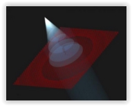
In another experiment, the team was able to use a metasurface to create a beam with radial polarization, that is, a beam whose polarization is pointing toward the beam axis. Such beams have doughnut-shaped intensity profiles and have applications in superresolution microscopy, laser cutting, and particle acceleration. "You generally would need a large optical setup, consisting of multiple components, to create this effect using conventional instruments," Arbabi says. "With our setup, we can compress all of the optical components into one device and generate these beams with higher efficiency and more purity."
The team is currently working with industrial partners to create metasurfaces for use in commercial devices such as miniature cameras and spectrometers, but a limited number have already been produced for use in optical experiments by collaborating scientists in other disciplines.
In addition, the Faraon lab current is investigating ways to combine different metasurfaces to create functioning optical systems and to correct for color distortions and other optical aberrations. "Like any optical system, you get distortions," Faraon said. "That's why expensive cameras have multiple lenses inside. Right now, we are experimenting with stacking different metasurfaces to correct for these aberrations and achieve novel functionalities."
Share on:


Testimonial
"We’re proud to call I-Connect007 a trusted partner. Their innovative approach and industry insight made our podcast collaboration a success by connecting us with the right audience and delivering real results."
Julia McCaffrey - NCAB GroupSuggested Items
India’s Aerospace and Defence Engineered for Power, Driven by Electronics
09/16/2025 | Gaurab Majumdar, Global Electronics AssociationWith a defence budget of $82.05 billion (2025–26) and a massive $223 billion earmarked for aerospace and defence spending over the next decade, India is rapidly positioning itself as a major player in the global defence and aerospace market.
VIDEOTON EAS's Bulgarian Subsidiary Expands Into Automotive Products
09/15/2025 | VideotonVEAS Bulgaria, engaged in electronics manufacturing, has joined the ranks of VIDEOTON companies authorized to produce automotive products.
Variosystems Strengthens North American Presence with Southlake Relaunch 2025
09/15/2025 | VariosystemsVariosystems celebrated the relaunch of its U.S. facility in Southlake, Texas. After months of redesign and reorganization, the opening marked more than just the return to a modernized production site—it was a moment to reconnect with our teams, partners, and the local community.
Hanwha Aerospace to Collaborate with BAE Systems on Advanced Anti-jamming GPS for Guided Missiles
09/15/2025 | HanwhaHanwha Aerospace has signed a contract with BAE Systems to integrate next-generation, anti-jamming Global Positioning System (GPS) technology into Hanwha Aerospace’s Deep Strike Capability precision-guided weapon system.
EV Group Achieves Breakthrough in Hybrid Bonding Overlay Control for Chiplet Integration
09/12/2025 | EV GroupEV Group (EVG), a leading provider of innovative process solutions and expertise serving leading-edge and future semiconductor designs and chip integration schemes, today unveiled the EVG®40 D2W—the first dedicated die-to-wafer overlay metrology platform to deliver 100 percent die overlay measurement on 300-mm wafers at high precision and speeds needed for production environments. With up to 15X higher throughput than EVG’s industry benchmark EVG®40 NT2 system designed for hybrid wafer bonding metrology, the new EVG40 D2W enables chipmakers to verify die placement accuracy and take rapid corrective action, improving process control and yield in high-volume manufacturing (HVM).