


 Dan’s Biz Bookshelf: Four Important Books You Need to Read (Not Just Say You Have)
 The Marketing Minute: Cracking the Code of Technical Marketing


UT Researchers Give Nanosheets Local Magnetic Properties
September 10, 2015 | University of TwenteEstimated reading time: 3 minutes
Two-dimensional crystals are very suitable for creating high-quality magnetic thin films. This appears from two recent publications written by scientists from the University of Twente's MESA+ research institute. The researchers show that by growing the magnetic layers on various 2D crystals, better known as nanosheets, you can control the preferred direction of the magnetism very locally. In an article published in Advanced Functional Materials, they present this method to create magnetic patterns on the micrometer scale. In Angewandte Chemie, they demonstrate that you can make the nanosheets in less than a minute, while the synthesis process had been known to be very slow. The magnetic films can be deployed for many different applications, such as new generations of smartphones.
With pulsed laser deposition (PLD) you can achieve controlled growth of thin layers of certain materials. Here, a material is heated rapidly with a powerful laser beam, so that it evaporates and a plasma is created. This spreads quickly in a vacuum chamber and is deposited on a substrate where it forms a thin layer. In this way you can control the thickness of the layer and you can form smooth and thin layers, often with special properties that are interesting for use in electronics and electro-mechanics, for example. For such applications, it is however essential that you can also make patterns in the layered materials. This is not easy, especially because the substrate needs to be heated to temperatures above 500° C during the PLD process. Many of the existing methods are therefore not adapted to existing manufacturing methods for microstructures.
Use of nanosheets
The UT researchers have now developed a new method, in which they make use of nanosheets obtained from three-dimensional crystals with a layered structure. If you dissolve these crystals in a special liquid, they spontaneously disintegrate into individual nanosheets. It was long thought that the crystal disintegration process could take weeks. However, the researchers have now shown that the nanosheetsare already able to form within a few seconds, which opens the way for the production of nanosheets on a large scale.
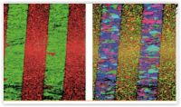
Based on the solution, various nanosheetscan be introduced in micro-patterns on a substrate. These patterns form the starting point for the growth of thin magnetic layers of magnetic LaSrMnO3 at high temperatures by means of PLD. Depending on the type of nanosheet the structure of the magnetic film assumes a specific orientation, and thus determines the magnetism of the film at that location. The process is monitored by means of, for example, electron backscatter diffraction (EBSD); a technique that makes it possible to 'reveal' the structure in the patterns.
Caption: EBSD image showing the local structure of a thin film. The left half of these images shows the preferred direction of the LaSrMnO3-film perpendicular to the growth direction, while the right half shows the directions in the plane with the contours of the individual nanosheets clearly visible. The distance between two lines in the pattern is a few micrometers.
Functional properties
The researchers show that you can use the micro patterns to control the functional properties of a material in detail. In addition to magnetism, it is possible to pattern other properties at the micrometer scale. An important step has thus been taking in bridging the gap between scientific research into artificial layered crystals and their ultimate application. The group from Twente plays a leading role in this worldwide.
Research
The research was performed by scientists from the Inorganic Materials Science department of UT research institute MESA+. It forms part of the TOP project funded by the Netherlands Organisation for Scientific Research (NWO) and the Chinese Scholarship Council. The research involved close cooperation with the Condensed-Matter and Medical Physics group at the University of California (UC, Irvine).
Share on:


Testimonial
"We’re proud to call I-Connect007 a trusted partner. Their innovative approach and industry insight made our podcast collaboration a success by connecting us with the right audience and delivering real results."
Julia McCaffrey - NCAB GroupSuggested Items
Alternative Manufacturing, Inc. (AMI) Announces Commitment to Excellence in Industrial, Defense, Aerospace, Renewables, and Robotics Markets
09/16/2025 | Alternative Manufacturing, Inc.Alternative Manufacturing, Inc. (AMI), a 100% employee-owned contract manufacturer, proudly reaffirms its leadership in the electronics manufacturing services (EMS) industry with a continued commitment to delivering high-quality PCBAs and box builds across the industrial, defense, aerospace, renewable energy, and robotics markets.
Sustainability and Selective Soldering
09/15/2025 | Dr. Samuel J. McMaster, Pillarhouse InternationalSustainability is more than just a buzzword for the electronics industry; it’s a key goal for all manufacturing processes. This is more than a box-ticking exercise or simply doing a small part for environmentally friendly processes. Moving toward sustainable solutions drives innovation and operational efficiency.
Trouble in Your Tank: Implementing Direct Metallization in Advanced Substrate Packaging
09/15/2025 | Michael Carano -- Column: Trouble in Your TankDirect metallization systems based on conductive graphite are gaining popularity throughout the world. The environmental and productivity gains achievable with this process are outstanding. Direct metallization reduces the costs of compliance, waste treatment, and legal issues related to chemical exposure. A graphite-based direct plate system has been devised to address these needs.
EV Group Achieves Breakthrough in Hybrid Bonding Overlay Control for Chiplet Integration
09/12/2025 | EV GroupEV Group (EVG), a leading provider of innovative process solutions and expertise serving leading-edge and future semiconductor designs and chip integration schemes, today unveiled the EVG®40 D2W—the first dedicated die-to-wafer overlay metrology platform to deliver 100 percent die overlay measurement on 300-mm wafers at high precision and speeds needed for production environments. With up to 15X higher throughput than EVG’s industry benchmark EVG®40 NT2 system designed for hybrid wafer bonding metrology, the new EVG40 D2W enables chipmakers to verify die placement accuracy and take rapid corrective action, improving process control and yield in high-volume manufacturing (HVM).
Integrating Uniplate PLBCu6 With the Digital Factory Suite
09/12/2025 | Giovanni Obino and Andreas Schatz, MKS' AtotechPrinted circuit board manufacturing is rapidly changing, driven by miniaturization, stringent reliability requirements, and growing pressure for sustainable production. Meeting these challenges requires more than incremental improvements; it demands a combination of precise equipment and real-time process intelligence. The pairing of Uniplate® PLBCu6 with the Digital Factory Suite (DFS) demonstrates how hardware and software can work together to create more responsive, resource-efficient manufacturing.