


 Dan’s Biz Bookshelf: Four Important Books You Need to Read (Not Just Say You Have)
 The Marketing Minute: Cracking the Code of Technical Marketing


Evidence of High-Temperature Superconductivity in Single Layer Unveiled
October 2, 2015 | ORNLEstimated reading time: 2 minutes
Electron microscopy at the Department of Energy’s Oak Ridge National Laboratory is pointing researchers closer to the development of ultra-thin materials that transfer electrons with no resistance at relatively high temperatures.
The study delivers direct evidence of high-temperature superconductivity at the interface of two insulating oxide materials. The paper by researchers from ORNL and the University of Rome Tor Vergata (Italy) is published in Physical Review Letters.
“One grand challenge in science is to manipulate materials locally by changing the distribution of atoms and the electronic structure, and that’s what we’re doing here,” Cantoni said. “This is a way to control the material – by manipulating the oxygen to make this interface superconducting.”
The ability to control and confine a material’s superconductivity could lead to two-dimensional superconductors for applications such as increasingly smaller computing technologies.
“We always want to scale down to get functionality in thinnest amount of material possible,” Cantoni said. “Usually when a material becomes thinner and thinner, its superconductivity disappears.”
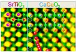
In the PRL study, researchers used scanning transmission electron microscopy at ORNL to examine the interface between two insulators, calcium copper oxide and strontium titanate oxide. The resulting data, combined with electron energy loss spectroscopy, confirmed that high-temperature superconductivity occurs within a highly confined region around the interface.
“We were able to establish that a one-unit-cell-thick calcium copper oxide layer at this interface is superconducting and that the critical temperature approaches 50 Kelvin, which is considered high temperature superconductivity,” Cantoni said.
The team’s microscopy showed that superconductivity arises from oxygen ions that are incorporated into the interface calcium layer during the growth process. The extra oxygen ions pull electrons from the adjacent copper oxide layer, creating holes known to produce superconductivity.
The study is published as “High Tc superconductivity at the interface between the CaCuO2 and SrTiO3 insulating oxides.” Coauthors include University of Rome Tor Vergata’s D. Di Castro, F. Ridolfi, C. Aruta, A. Tebano, N. Yang, and G. Balestrino.
The research was supported in part by DOE’s Office of Science (Basic Energy Sciences) and used resources of the Center for Nanophase Materials Sciences, a DOE Office of Science User Facility at ORNL.
ORNL is managed by UT-Battelle for the Department of Energy’s Office of Science.
DOE’s Office of Science is the single largest supporter of basic research in the physical sciences in the United States, and is working to address some of the most pressing challenges of our time. For more information, please visit science.energy.gov.
Share on:


Testimonial
"The I-Connect007 team is outstanding—kind, responsive, and a true marketing partner. Their design team created fresh, eye-catching ads, and their editorial support polished our content to let our brand shine. Thank you all! "
Sweeney Ng - CEE PCBSuggested Items
Electrodeposited Copper Foils Market to Grow by $11.7 Billion Over 2025-2032
09/18/2025 | Globe NewswireThe global electrodeposited copper foils market is poised for dynamic growth, driven by the rising adoption in advanced electronics and renewable energy storage solutions.
MacDermid Alpha Showcases Advanced Interconnect Solutions at PCIM Asia 2025
09/18/2025 | MacDermid Alpha Electronics SolutionsMacDermid Alpha Electronic Solutions, a global leader in materials for power electronics and semiconductor assembly, will showcase its latest interconnect innovations in electronic interconnect materials at PCIM Asia 2025, held from September 24 to 26 at the Shanghai New International Expo Centre, Booth N5-E30
Trouble in Your Tank: Implementing Direct Metallization in Advanced Substrate Packaging
09/15/2025 | Michael Carano -- Column: Trouble in Your TankDirect metallization systems based on conductive graphite are gaining popularity throughout the world. The environmental and productivity gains achievable with this process are outstanding. Direct metallization reduces the costs of compliance, waste treatment, and legal issues related to chemical exposure. A graphite-based direct plate system has been devised to address these needs.
Closing the Loop on PCB Etching Waste
09/09/2025 | Shawn Stone, IECAs the PCB industry continues its push toward greener, more cost-efficient operations, Sigma Engineering’s Mecer System offers a comprehensive solution to two of the industry’s most persistent pain points: etchant consumption and rinse water waste. Designed as a modular, fully automated platform, the Mecer System regenerates spent copper etchants—both alkaline and acidic—and simultaneously recycles rinse water, transforming a traditionally linear chemical process into a closed-loop system.
Driving Innovation: Depth Routing Processes—Achieving Unparalleled Precision in Complex PCBs
09/08/2025 | Kurt Palmer -- Column: Driving InnovationIn PCB manufacturing, the demand for increasingly complex and miniaturized designs continually pushes the boundaries of traditional fabrication methods, including depth routing. Success in these applications demands not only on robust machinery but also sophisticated control functions. PCB manufacturers rely on advanced machine features and process methodologies to meet their precise depth routing goals. Here, I’ll explore some crucial functions that empower manufacturers to master complex depth routing challenges.