


 Dan’s Biz Bookshelf: Four Important Books You Need to Read (Not Just Say You Have)
 The Marketing Minute: Cracking the Code of Technical Marketing


Molecular Nanoribbons as Electronic Highways
October 6, 2015 | Umeå UniversityEstimated reading time: 2 minutes
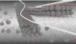
Physicists at Umeå University have, together with researchers at UC Berkeley, USA, developed a method to synthesise a unique and novel type of material which resembles a graphene nanoribbon but in molecular form. This material could be important for the further development of organic solar cells.
The nanoribbons are comprised of molecules with the chemical formula [6,6]-phenyl-C61-butyric acid methyl ester. For short it is denoted PCBM, and in practice it is a fullerene molecule (a football-shaped carbon molecule) with an attached side arm to increase its solubility. PCBM molecules are commonly used in organic solar cells since they have a very good ability to transport free electrons that are "generated" by solar light.
The researchers at Umeå University and UC Berkeley have now developed a method to arrange such molecules into thin, crystalline nanoribbons that are only four nanometres wide. The nanoribbons are grown in a solution process with quite high efficiency and all nanoribbons have a unique morphology with edges in a zigzag.
"It is a very intriguing material and the method is quite simple. The material resembles the more commonly known graphene nanoribbons, but in our material each carbon atom is 'replaced' by a molecule," says Thomas Wågberg, associate professor at the Department of Physics, who has led the study.
The findings are interesting for several reasons; it is the first time that structures with so small dimensions have been produced with this type of molecule, and the dimensions of the nanoribbons suggest that they should be ideal as "electronic highways" in organic solar cells. An organic solar cell usually consists of two types of material, one that conducts the electrons and one that conducts the "holes" that are left behind when the electron gets an energy boost from the incoming solar light (you can see the transport of "hole" as an empty space in traffic moving backwards in a traffic queue moving forwards).
An electron conductor in organic solar cells should ideally form long pathways to the electrode but concurrently be thinner than 10-15 nanometres (approximately 10,000 times the thickness of a normal hair). The newly developed PCBM nanoribbons fulfil all these requirements.
"Together with professor Ludvig Edman's group at the Department of Physics at Umeå University, we are now investigating this material further as a potential component in organic solar cells in the hope of making such devices more efficient," says Thomas Wågberg.
Our study is of course also interesting for fundamental reasons since it opens up possibilities to investigate important physical properties of molecular materials with nanoscale dimensions.
About nanoribbons:
Carbon nanostructures exist in many different forms. Graphene is a single layer of carbon atoms, which can be "ripped" into nanoribbons under certain circumstances. Due to the decrease in dimensions along one direction, the graphene nanoribbons display many unique properties. Fullerenes on the other hand are football-shaped molecules also built up from carbon atoms, while PCBM are fullerene-like molecules with several interesting properties and an attached side arm to increase their solubility. In the current study the researchers have been able to construct nanoribbons comprising PCBM molecules instead of carbon atoms, so that the structure strongly resembles a graphene nanoribbon in molecular form.
Share on:


Testimonial
"Advertising in PCB007 Magazine has been a great way to showcase our bare board testers to the right audience. The I-Connect007 team makes the process smooth and professional. We’re proud to be featured in such a trusted publication."
Klaus Koziol - atgSuggested Items
Curing and Verification in PCB Shadow Areas
09/17/2025 | Doug Katze, DymaxDesign engineers know a simple truth that often complicates electronics manufacturing: Light doesn’t go around corners. In densely populated PCBs, adhesives and coatings often fail to fully cure in shadowed regions created by tall ICs, connectors, relays, and tight housings.
Marcy’s Musings: Advancing the Advanced Materials Discussion
09/17/2025 | Marcy LaRont -- Column: Marcy's MusingsAs the industry’s most trusted global source of original content about the electronics supply chain, we continually ask you about your concerns, what you care about, and what you most want to learn about. Your responses are insightful and valuable. Thank you for caring enough to provide useful feedback and engage in dialogue.
September 2025 PCB007 Magazine: The Future of Advanced Materials
09/16/2025 | I-Connect007 Editorial TeamMoore’s Law is no more, and the advanced material solutions being developed to grapple with this reality are surprising, stunning, and perhaps a bit daunting. Buckle up for a dive into advanced materials and a glimpse into the next chapters of electronics manufacturing.
I-Connect007 Launches Advanced Electronics Packaging Digest
09/15/2025 | I-Connect007I-Connect007 is pleased to announce the launch of Advanced Electronics Packaging Digest (AEPD), a new monthly digital newsletter dedicated to one of the most critical and rapidly evolving areas of electronics manufacturing: advanced packaging at the interconnect level.
Panasonic Industry will Double the Production Capacity of MEGTRON Multi-layer Circuit Board Materials Over the Next Five Years
09/15/2025 | Panasonic Industry Co., Ltd.Panasonic Industry Co., Ltd., a Panasonic Group company, announced plans for a major expansion of its global production capacity for MEGTRON multi-layer circuit board materials today. The company plans to double its production over the next five years to meet growing demand in the AI server and ICT infrastructure markets.