


 Dan’s Biz Bookshelf: Four Important Books You Need to Read (Not Just Say You Have)
 The Marketing Minute: Cracking the Code of Technical Marketing


Measuring the Behavior of Specific Atoms in Dielectric Materials
October 14, 2015 | NC State UniversityEstimated reading time: 3 minutes
Researchers from North Carolina State University, the National Institute of Standards and Technology (NIST), and UNSW Australia have measured the behavior of specific atoms in dielectric materials when exposed to an electric field. The work advances our understanding of dielectric materials, which are used in a wide variety of applications – from handheld electronics to defibrillators.
“Dielectric materials are insulators that can store and manage electric charge. But we hadn’t yet directly measured how atoms move in dielectric materials in order to store that charge,” says Tedi-Marie Usher, a Ph.D. candidate in materials science and engineering at NC State and lead author of a paper on the work.
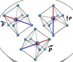
Researchers have measured how the atoms within electrically insulating solids reorient due to an applied electric field. Shown here for Na1/2Bi1/2TiO3, bismuth ions (purple) align along the electric field direction relative to their surrounding titanium ions (blue). Oxygen ions not shown.
To get to the bottom of this problem, the researchers applied voltage to a dielectric material, creating an electric field. They simultaneously bombarded the material with X-rays from a synchrotron at Argonne National Laboratory’s Advanced Photon Source. When the X-rays hit the material, they scatter into a pattern of bright rings. Typically, to figure out the arrangement of atoms in a material, the positions and intensities of these bright rings are analyzed.
However, by applying new mathematical techniques that are more sensitive to the weak (dim) scattered X-rays, the researchers could determine changes in the placement of specific atoms within the crystalline structure of the material. In other words, the researchers could “see” how the atoms moved relative to each other in response to the electric field.
“A good analogy would be that analyzing the bright rings is like examining a skyscraper from far away and determining that each office is 500 square feet. However, by also analyzing the weak X-rays scattered from the sample, we can determine that some offices are 400 square feet and others are 600 square feet, and some have the desk on the east side, and others have the desk on the north side,” says Usher. This is an uncommon approach, because experimenters typically only evaluate the bright rings.
“What’s really new here is that this technique is much more sensitive to the behavior of select atoms relative to their neighboring atoms, rather than looking at an average of all the atoms in a sample,” says Jacob Jones, a professor of materials science and engineering at NC State and corresponding author of the paper.
The work uses a technique called a pair distribution function, which allows researchers to extract information about how atoms are arranged at extremely small length-scales based on the weak intensity X-rays diffracted from a sample. The researchers evaluated three different dielectric materials for this study.
“One of the interesting findings here is that each of the three dielectric materials we tested exhibited very different behaviors at the atomic level – there was no single atomic behavior that accounted for dielectric properties across the materials,” Jones says.
For example, the researchers tested a material called sodium bismuth titanate – a non-toxic material that is thought to be promising for use in dielectric devices. In the absence of an electric field, researchers knew that the bismuth ions are off-center relative to neighboring atoms. But different bismuth ions would be off-center in different directions. However, when an electric field is applied, virtually all of the bismuth ions shifted so they were off-center in the same direction as the electric field.
“Neither of the other dielectric materials exhibited similar behavior,” Usher says. “One of our questions for future work is whether the bismuth behavior we saw in sodium bismuth titanate is consistent across bismuth-based dielectrics.”
“We also want to know how dielectric materials and other complex materials, such as high-entropy alloys, behave at the atomic scale when under mechanical stress,” Jones says.
Share on:


Testimonial
"Our marketing partnership with I-Connect007 is already delivering. Just a day after our press release went live, we received a direct inquiry about our updated products!"
Rachael Temple - AlltematedSuggested Items
Curing and Verification in PCB Shadow Areas
09/17/2025 | Doug Katze, DymaxDesign engineers know a simple truth that often complicates electronics manufacturing: Light doesn’t go around corners. In densely populated PCBs, adhesives and coatings often fail to fully cure in shadowed regions created by tall ICs, connectors, relays, and tight housings.
Marcy’s Musings: Advancing the Advanced Materials Discussion
09/17/2025 | Marcy LaRont -- Column: Marcy's MusingsAs the industry’s most trusted global source of original content about the electronics supply chain, we continually ask you about your concerns, what you care about, and what you most want to learn about. Your responses are insightful and valuable. Thank you for caring enough to provide useful feedback and engage in dialogue.
September 2025 PCB007 Magazine: The Future of Advanced Materials
09/16/2025 | I-Connect007 Editorial TeamMoore’s Law is no more, and the advanced material solutions being developed to grapple with this reality are surprising, stunning, and perhaps a bit daunting. Buckle up for a dive into advanced materials and a glimpse into the next chapters of electronics manufacturing.
I-Connect007 Launches Advanced Electronics Packaging Digest
09/15/2025 | I-Connect007I-Connect007 is pleased to announce the launch of Advanced Electronics Packaging Digest (AEPD), a new monthly digital newsletter dedicated to one of the most critical and rapidly evolving areas of electronics manufacturing: advanced packaging at the interconnect level.
Panasonic Industry will Double the Production Capacity of MEGTRON Multi-layer Circuit Board Materials Over the Next Five Years
09/15/2025 | Panasonic Industry Co., Ltd.Panasonic Industry Co., Ltd., a Panasonic Group company, announced plans for a major expansion of its global production capacity for MEGTRON multi-layer circuit board materials today. The company plans to double its production over the next five years to meet growing demand in the AI server and ICT infrastructure markets.