


 Dan’s Biz Bookshelf: Four Important Books You Need to Read (Not Just Say You Have)
 The Marketing Minute: Cracking the Code of Technical Marketing


Electronics Get a Power Boost with the Addition of a Simple Material
October 20, 2015 | Pennsylvania State UniversityEstimated reading time: 4 minutes
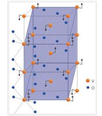
The tiny transistor is the heart of the electronics revolution, and Penn State materials scientists have just discovered a way to give this workhorse a big boost, using a new technique to incorporate vanadium oxide -- a functional oxide -- into the electronic devices.
"It's tough to replace current transistor technology because semiconductors do such a fantastic job," said Roman Engel-Herbert, assistant professor of materials science and engineering. "But there are some materials, like vanadium oxide, that you can add to existing devices to make them perform even better."
The researchers knew that vanadium dioxide, which is just a specific combination of the elements vanadium and oxygen, had an unusual property called the metal-to-insulator transition. In the metal state, electrons move freely, while in the insulator state, electrons cannot flow. This on/off transition, inherent to vanadium dioxide, is also the basis of computer logic and memory.
The researchers thought that if they could add vanadium oxide close to a device's transistor it could boost the transistor's performance. Also, by adding it to the memory cell, it could improve the stability and energy efficiency to read, write and maintain the information state. The major challenge they faced was that vanadium dioxide of sufficiently high quality had never been grown in a thin film form on the scale required to be of use to industry -- the wafer scale.
Although vanadium dioxide, the targeted compound, looks simple, it is very difficult to synthesize. In order to create a sharp metal-to-insulator transition, the ratio of vanadium to oxygen needs to be precisely controlled. When the ratio is exactly right, the material will show more than four orders-of-magnitude change in resistance, enough for a sufficiently strong on/off response.
The Penn State team reports in the online journal Nature Communications that they are the first to achieve growth of thin films of vanadium dioxide on 3-inch sapphire wafers with a perfect 1 to 2 ratio of vanadium to oxygen across the entire wafer. The material can be used to make hybrid field effect transistors, called hyper-FETs, which could lead to more energy efficient transistors. Earlier this year, also in Nature Communications, a research group led by Suman Datta, professor of electrical and electronic engineering, Penn State, showed that the addition of vanadium dioxide provided steep and reversible switching at room temperature, reducing the effects of self-heating and lowering the energy requirements of the transistor.
The implementation of vanadium dioxide can also benefit existing memory technologies, a quest that Penn State researchers are actively pursuing.
"The metal-to-insulator property of vanadium dioxide can ideally enhance state-of-the-art non-volatile memories by using the material as an augmentation device, which, interestingly, can also serve as a selector in some memory architecture," said Sumeet Gupta, Monkowski Assistant Professor of Electrical Engineering and group leader of the Integrated Circuits and Devices Lab, Penn State.
A selector insures that reading or writing information on a memory chip is done within a single memory cell, without bleeding over into neighboring cells. The selector works by changing the resistivity of the cell, which vanadium dioxide does extremely well. In addition, the change in resistivity of vanadium oxide can be used to significantly increase the robustness of the read operation.
"To determine the right ratio of vanadium to oxygen, we applied an unconventional approach in which we simultaneously deposit vanadium oxide with varying vanadium-to-oxygen ratios across the sapphire wafer," said Hai-Tian Zhang, Ph.D. student in Engel-Herbert's group. "Using this 'library' of vanadium-to-oxygen ratios, we can perform flux calculations to determine the optimal combination that would give an ideal 1 to 2 vanadium to oxygen ratio in the film. This new method will allow a rapid identification of the optimal growth condition for industrial applications, avoiding a long and tedious series of trial-and-error experiments."
The vanadium dioxide thin-film material grown with this method was used to make super-high-frequency switches, in collaboration with the Datta group at Penn State and Notre Dame, a technology important in communications. These switches show cut-off frequencies an order of magnitude higher than conventional devices. This work will be reported at the IEEE International Electron Device Meeting, the leading forum for reporting technological breakthroughs in the semiconductor and electronic device industry, in December.
"We are starting to realize that the class of materials exhibiting these on/off responses can be beneficial in various ways in information technology, such as increasing the robustness and energy efficiency of read/write and compute operations in memory, logic and communication devices," Engel-Herbert said. "When you can make high-quality vanadium dioxide on a wafer scale, people are going to have many excellent ideas on how it can be used."
Other researchers on this project were graduate students Lei Zhang, Debangshu Mukherjee, Ryan Haislmaier, and assistant professor Nasim Alem all in the Department of Materials Science and Engineering and the Materials Research Institute at Penn State, and Yuan-Xia Zheng, a graduate student in Physics.
The National Science Foundation and the Penn State Center for Nanoscale Science supported this work. Analysis and measurement was performed in the Penn State Materials Characterization Laboratory, a facility of the Materials Research Institute.
Share on:


Testimonial
"Advertising in PCB007 Magazine has been a great way to showcase our bare board testers to the right audience. The I-Connect007 team makes the process smooth and professional. We’re proud to be featured in such a trusted publication."
Klaus Koziol - atgSuggested Items
Curing and Verification in PCB Shadow Areas
09/17/2025 | Doug Katze, DymaxDesign engineers know a simple truth that often complicates electronics manufacturing: Light doesn’t go around corners. In densely populated PCBs, adhesives and coatings often fail to fully cure in shadowed regions created by tall ICs, connectors, relays, and tight housings.
Marcy’s Musings: Advancing the Advanced Materials Discussion
09/17/2025 | Marcy LaRont -- Column: Marcy's MusingsAs the industry’s most trusted global source of original content about the electronics supply chain, we continually ask you about your concerns, what you care about, and what you most want to learn about. Your responses are insightful and valuable. Thank you for caring enough to provide useful feedback and engage in dialogue.
September 2025 PCB007 Magazine: The Future of Advanced Materials
09/16/2025 | I-Connect007 Editorial TeamMoore’s Law is no more, and the advanced material solutions being developed to grapple with this reality are surprising, stunning, and perhaps a bit daunting. Buckle up for a dive into advanced materials and a glimpse into the next chapters of electronics manufacturing.
I-Connect007 Launches Advanced Electronics Packaging Digest
09/15/2025 | I-Connect007I-Connect007 is pleased to announce the launch of Advanced Electronics Packaging Digest (AEPD), a new monthly digital newsletter dedicated to one of the most critical and rapidly evolving areas of electronics manufacturing: advanced packaging at the interconnect level.
Panasonic Industry will Double the Production Capacity of MEGTRON Multi-layer Circuit Board Materials Over the Next Five Years
09/15/2025 | Panasonic Industry Co., Ltd.Panasonic Industry Co., Ltd., a Panasonic Group company, announced plans for a major expansion of its global production capacity for MEGTRON multi-layer circuit board materials today. The company plans to double its production over the next five years to meet growing demand in the AI server and ICT infrastructure markets.