


 American Made Advocacy: Five Years of Educating, Advocating, and Influencing Legislation and Policy
 Defense Speak Interpreted: Understanding What the Department of Defense Is, and Isn’t
 The Right Approach: The End of an Era—DoD Proposes MIL-PRF-31032 Cancellation


Future integrated circuitry is expected to look a lot like skyscrapers: units will be stacked atop one another and interconnects will link each level to its adjacent neighbors, much like how elevators connect one floor to the next. The problem is how do integrated-circuit designers remove heat from these tightly packed 3-D chips? The smaller the space between the chips, the harder it is to remove the heat.
Although circuit designers are still working the challenge for commercial applications, the problem poses an especially difficult conundrum for those designing 3-D integrated circuitry for space-based uses.
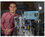
Because of the unique space environment, removing heat from power-dense electronics always has presented challenges, sometimes leading to inefficient designs, said Franklin Robinson, a NASA thermal engineer at the agency's Goddard Space Flight Center in Greenbelt, Maryland. He and his team are studying different cooling techniques so that NASA might benefit from this emerging technology in the future.
“These 3-D-stacked integrated circuits are coming; they will be commercialized. We need to get ahead of the curve when they do become available,” Robinson said.
He’s not alone in his enthusiasm for the new-fangled technology. The thirst for more features and computing power has driven the electronics industry to adopt 3-D integrated-circuit technology. Though manufacturing and technical challenges remain, the emerging technology promises to save space in future electronic devices and instruments — chips are stacked atop each other and not spread over a circuit board. With shorter wiring linking the chips, data would move both horizontally and vertically, improving bandwidth, computational speed and performance, all while consuming less power.
Greater functionality in a smaller package is especially important to NASA, Robinson said. “Miniature instruments are vital to NASA’s emerging mission portfolio. The goal for these instruments is to provide the greatest functionality in the smallest package.”
Making Sure NASA Benefits
To make sure NASA benefits from this emerging 3-D-circuit technology, Robinson and his team have begun investigating a technology that would remove heat by flowing a coolant through embedded channels about the size of a human hair within or between the chips.
In contrast, removing heat in more traditional 2-D integrated circuits is significantly different, he explained. Designers create a “floor plan,” keeping the heat-generating devices as far apart as possible. The heat travels into the printed circuit board, where it is directed to a clamp in the sidewall of the electronics box, eventually making its way to a box-mounted radiator.
“This approach is not applicable to chip stacks because one or more of the chips in the stack is not in contact with the printed circuit board,” he said. “However, we can remove the heat by flowing a coolant through these tiny, embedded channels.”
To further improve the microchannel coolers, the team also is investigating the effectiveness of “flow boiling,” where the coolant boils as it flows through the tiny gaps. According to Robinson, the technique offers a higher rate of heat transfer, which keeps devices cooler and, therefore, less likely to fail due to overheating. It also relies on the working fluid’s latent heat of vaporization, which reduces the flow rate, minimizing pumping power.
Another potential benefit exists: flow boiling in miniature channels may not be affected by the lack of gravity, which is important when designing a technology that ultimately must fly in a low-gravity environment, he said.
Under his research, Robinson is evaluating two-phase flows in miniature channels, with the goal of producing a list of criteria for channel dimensions, flow parameters and fluid properties that produce gravity insensitivity.
“This is essential because some systems experience variations in performance with changes in gravity,” he said. “This is troublesome because in-orbit performance may not match terrestrial performance. By mapping the conditions that provide gravity-insensitivity, we can dramatically reduce the risk for space-based applications.”


