


 Dan’s Biz Bookshelf: ‘The Future of Sales'
 Driving Innovation: Traceability in PCB Production
 It’s Only Common Sense: Price—Is That All You’ve Got?


Economic LED Recycling
November 3, 2015 | Fraunhofer-GesellschaftEstimated reading time: 2 minutes
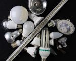
Light emitting diodes are used in a great number of products like televisions and lamps or luminaires. Moreover they are penetrating the automotive lighting market to an ever greater degree. Nevertheless, there are no suitable recycling processes available today for these items. Researchers have developed a method to mechanically separate LEDs.
Modern illuminants are manufactured using a variety of materials. The housing is made of glass or plastic, the heat sink consists of ceramic or aluminum, and the resistors and cables contain copper. The most valuable materials are found within the LEDs themselves. They are indium and gallium inside the semiconductor diode and rare earths like europium or terbium in the phosphor. This makes it relatively expensive to manufacture the diodes, and the margins are small. “Right now recyclers are starting to receive LED products, but currently they are often simply stored as there is no suitable recycling process available yet. The main goal is to recover the valuable materials. It’s only a matter of time until recyclers will have to start processing LEDs,” says Jörg Zimmermann from the Fraunhofer Project Group for Materials Recycling and Resource Strategies IWKS in Alzenau and Hanau of the Fraunhofer Institute for Silicate Research ISC.
Separating components with the help of shock waves
Using the “electrohydraulic comminution” process, researchers break the LED lamps into their constituent parts without destroying the LEDs themselves. Shock waves created by electrical impulses in a water bath separate the individual components at their predetermined break points. The components can then be recycled individually. The researchers have adapted their experimental setup to retrofit lamps, which resemble traditional light bulbs or fluorescent tubes and can be used in the same standard sockets. “This method works in principle also for other sizes, for instance with LEDs from television sets or with automobile headlights, as well as with other electronic products,” explains Zimmermann.
A prerequisite for an efficient recycling process is a neat separation of the components. “To efficiently separate and recycle all components of a LED lamp, an entirely different approach is necessary - one that produces large quantities of semiconductor and phosphor materials,” says Zimmermann. If the entire retrofit is shredded, it is much more difficult to separate the resulting mixture of materials. Breaking LED lamps down to the component level also makes it easier to recover greater quantities of the materials contained in them. This is accomplished by collecting large quantities of similar components in which the concentration of individual elements is already higher. Zimmermann clarifies that this reprocessing is only profitable for recyclers and manufacturers, if it involves larger quantities.
“We’re still testing whether the comminution process can be repeated until the desired materials have been separated,” says Zimmerman. The researchers can adjust the parameters of the experimental setup like the type and quantity of the fluid, the container size, or the electric pulse voltage in such a way that separation occurs precisely at the specified break points. “In particular it is the number of pulses that determines how the components will separate,” he says. The electrohydraulic comminution process is currently being investigated in detail and improved further, also to gain access to other LED application areas. “Our research has demonstrated that mechanical separation is a viable method for improving the economics of LED lamp recycling,” says Zimmermann.
Share on:


Suggested Items
RF PCB Design Tips and Tricks
05/08/2025 | Cherie Litson, EPTAC MIT CID/CID+There are many great books, videos, and information online about designing PCBs for RF circuits. A few of my favorite RF sources are Hans Rosenberg, Stephen Chavez, and Rick Hartley, but there are many more. These PCB design engineers have a very good perspective on what it takes to take an RF design from schematic concept to PCB layout.
Trouble in Your Tank: Causes of Plating Voids, Pre-electroless Copper
05/09/2025 | Michael Carano -- Column: Trouble in Your TankIn the business of printed circuit fabrication, yield-reducing and costly defects can easily catch even the most seasoned engineers and production personnel off guard. In this month’s column, I’ll investigate copper plating voids with their genesis in the pre-plating process steps.
Elephantech: For a Greener Tomorrow
04/16/2025 | Marcy LaRont, PCB007 MagazineNobuhiko Okamoto is the global sales and marketing manager for Elephantech Inc., a Japanese startup with a vision to make electronics more sustainable. The company is developing a metal inkjet technology that can print directly on the substrate and then give it a copper thickness by plating. In this interview, he discusses this novel technology's environmental advantages, as well as its potential benefits for the PCB manufacturing and semiconductor packaging segments.
Trouble in Your Tank: Organic Addition Agents in Electrolytic Copper Plating
04/15/2025 | Michael Carano -- Column: Trouble in Your TankThere are numerous factors at play in the science of electroplating or, as most often called, electrolytic plating. One critical element is the use of organic addition agents and their role in copper plating. The function and use of these chemical compounds will be explored in more detail.
IDTechEx Highlights Recyclable Materials for PCBs
04/10/2025 | IDTechExConventional printed circuit board (PCB) manufacturing is wasteful, harmful to the environment and energy intensive. This can be mitigated by the implementation of new recyclable materials and technologies, which have the potential to revolutionize electronics manufacturing.