


 Dan’s Biz Bookshelf: Four Important Books You Need to Read (Not Just Say You Have)
 The Marketing Minute: Cracking the Code of Technical Marketing


The Complexity of Modelling
November 4, 2015 | IUCREstimated reading time: 3 minutes
In recent years, advances in materials synthesis techniques have enabled scientists to produce increasingly complex functional materials with enhanced or novel macroscopic properties. For example, ultra-small core-shell metallic nanoparticles used for catalysis, high entropy alloys made of 6 or 7 elements to give high strength at high temperatures and pharmaceuticals engineered at the nano-scale for more effective drug delivery. Modern engineered materials drive progress in many scientific disciplines and are at the heart of next-generation technologies in industrial fields including electronics, energy production and storage, environmental engineering, and biomedicine. As the optical, electronic and mechanical properties of such materials are deeply influenced by atomic structure, solving the structure of engineered materials is of critical importance to unlocking their true potential.
However, the structures of such materials are often complex and non-periodic at the atomic scale or at the nanoscale. For example, many of the best known thermoelectric materials have structures that are crystallographic on average, but derive their high thermoelectric figure of merit from local atomic distortions. Disordered collections of nanoparticles, on the other hand, have a high degree of short- range order but no long-range order beyond the nanoscale. Additionally, many novel materials are composites, which exhibit complex ordering on multiple length scales, so the complexity faced by the materials scientist wishing to understand the structure of new and novel materials is considerable.
The standard techniques of crystallography have proven successful in characterizing a vast array of bulk materials whose atomic structures can be described with crystal models that require only tens or hundreds of parameters. Since X-ray diffraction data typically yield information on hundreds or thousands of diffraction peaks, a unique structure solution can almost always be found for crystalline materials. However, for the types of complex materials described above the number of degrees of freedom in suitable structure models is often considerably larger than in the case of a typical crystal. Additionally, complex engineered materials often produce extremely broad peaks in diffraction experiments, due to the fact that they are non-periodic or disordered. Thus, the structure problem is doubly complicated, as diffraction experiments produce less information than corresponding experiments on bulk materials. From a standard crystallographic perspective, the structure problem for many complex materials is inherently ill posed, making a unique solution impossible. When the standard techniques of crystallography fail, it is sometimes possible to develop new analytical tools to maximise the information extracted from a diffraction pattern, but even with such advances a unique solution can often not be found to a fundamentally ill-posed problem without defining new constraints or adding additional data.
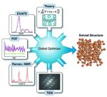
To obtain unique structure solutions for complex materials, a new paradigm of analysis is needed: a methodology that can combine different information sources and models into a coherent framework to solve problems using global optimisation. Within this framework, a material with unknown structure could be probed with various experimental tools, such as X-ray diffraction, transmission electron microscopy, small-angle X-ray or neutron scattering, Raman spectroscopy etc. to yield an array of data sets that would then be fed into a global optimiser. Additionally, theoretical inputs, such as density- functional theory could be integrated into the optimisation. While each single experimental or theoretical input may not generate enough information to produce a solution, together the pieces of information would regularise the problem, resulting in a unique solution.
A group of scientists from the United States of America [Juhás et al. (2015), Acta Cryst. A71, 562-568 provide a complete description of an implementation of complex modelling, one which is robust, modular and easily adaptable to different types of problems and different combinations of data sets and theoretical inputs. The key is to break the process down into its constituent parts, which can then be combined and linked as necessary to solve the problem at hand.
Share on:


Testimonial
"In a year when every marketing dollar mattered, I chose to keep I-Connect007 in our 2025 plan. Their commitment to high-quality, insightful content aligns with Koh Young’s values and helps readers navigate a changing industry. "
Brent Fischthal - Koh YoungSuggested Items
Curing and Verification in PCB Shadow Areas
09/17/2025 | Doug Katze, DymaxDesign engineers know a simple truth that often complicates electronics manufacturing: Light doesn’t go around corners. In densely populated PCBs, adhesives and coatings often fail to fully cure in shadowed regions created by tall ICs, connectors, relays, and tight housings.
Marcy’s Musings: Advancing the Advanced Materials Discussion
09/17/2025 | Marcy LaRont -- Column: Marcy's MusingsAs the industry’s most trusted global source of original content about the electronics supply chain, we continually ask you about your concerns, what you care about, and what you most want to learn about. Your responses are insightful and valuable. Thank you for caring enough to provide useful feedback and engage in dialogue.
September 2025 PCB007 Magazine: The Future of Advanced Materials
09/16/2025 | I-Connect007 Editorial TeamMoore’s Law is no more, and the advanced material solutions being developed to grapple with this reality are surprising, stunning, and perhaps a bit daunting. Buckle up for a dive into advanced materials and a glimpse into the next chapters of electronics manufacturing.
I-Connect007 Launches Advanced Electronics Packaging Digest
09/15/2025 | I-Connect007I-Connect007 is pleased to announce the launch of Advanced Electronics Packaging Digest (AEPD), a new monthly digital newsletter dedicated to one of the most critical and rapidly evolving areas of electronics manufacturing: advanced packaging at the interconnect level.
Panasonic Industry will Double the Production Capacity of MEGTRON Multi-layer Circuit Board Materials Over the Next Five Years
09/15/2025 | Panasonic Industry Co., Ltd.Panasonic Industry Co., Ltd., a Panasonic Group company, announced plans for a major expansion of its global production capacity for MEGTRON multi-layer circuit board materials today. The company plans to double its production over the next five years to meet growing demand in the AI server and ICT infrastructure markets.