


 Dan’s Biz Bookshelf: Four Important Books You Need to Read (Not Just Say You Have)
 The Marketing Minute: Cracking the Code of Technical Marketing


Researchers Create Cheaper High Performing LED
November 19, 2015 | Florida State UniversityEstimated reading time: 3 minutes
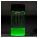
A team of Florida State University materials researchers has developed a new type of light-emitting diode, or LED, using an organic-inorganic hybrid that could lead to cheaper, brighter and mass produced lights and displays in the future.
Assistant Professor of Physics Hanwei Gao and Associate Professor of Chemical Engineering Biwu Ma are using a class of materials called organometal halide perovskites to build a highly functioning LED. They lay out their findings in the journal Advanced Materials.
“Early work suggested perovskites could be a promising material to build LEDs,” Gao said. “But, the performance was not up to their potential. We believed there was significant room for improvement.”
Perovskites are any materials with the same type of crystal structure as calcium titanium oxide. Other researchers experimented with perovskites to build LEDs in the past but could not build particularly effective ones. Gao and Ma believed this organic-inorganic hybrid could perform better, if the formula could be appropriately tweaked.
“When we thought about this class of material, we knew it should perform better than this,” Ma said. “We came up with our novel approach to solve some critical problems and get a high-performance LED.”
After months of experiments using synthetic chemistry to fine-tune the material properties and device engineering to control the device architectures, they ultimately created an LED that performed even better than expected.
The material glowed exceptionally bright.
It is measured at about 10,000 candelas per square meter at a driving voltage of 12V — candelas are the unit of measurement for luminescence. As a benchmark, LEDs glowing at about 400 candelas per square meter are sufficiently bright for computer screens.
“Such exceptional brightness is, to a large extent, owing to the inherent high luminescent efficiency of this surface-treated, highly crystalline nanomaterial,” Gao said.
It was also quick and easy to produce.
Gao and Ma can produce the material in about an hour in the lab and have a full device created and tested in about half a day.
Additionally, while bare hybrid perovskites tend to be unstable in humid air, the nanostructured perovskites exhibit remarkable stability in ambient environment because of the purposely designed surface chemistry. Such chemical stability largely reduces the requirement of sophisticated infrastructure to produce this new type of LEDs and could be of huge benefit for cost-effective manufacturing in the future.
The research is crucial to the advance of LED technology, which is fast becoming an avenue to reduce the country’s electric consumption. LED lighting is already sold in stores, but widespread adoption has been slow because of the costs associated with the material and the quality.
Page 1 of 2
Share on:


Testimonial
"In a year when every marketing dollar mattered, I chose to keep I-Connect007 in our 2025 plan. Their commitment to high-quality, insightful content aligns with Koh Young’s values and helps readers navigate a changing industry. "
Brent Fischthal - Koh YoungSuggested Items
Curing and Verification in PCB Shadow Areas
09/17/2025 | Doug Katze, DymaxDesign engineers know a simple truth that often complicates electronics manufacturing: Light doesn’t go around corners. In densely populated PCBs, adhesives and coatings often fail to fully cure in shadowed regions created by tall ICs, connectors, relays, and tight housings.
Marcy’s Musings: Advancing the Advanced Materials Discussion
09/17/2025 | Marcy LaRont -- Column: Marcy's MusingsAs the industry’s most trusted global source of original content about the electronics supply chain, we continually ask you about your concerns, what you care about, and what you most want to learn about. Your responses are insightful and valuable. Thank you for caring enough to provide useful feedback and engage in dialogue.
September 2025 PCB007 Magazine: The Future of Advanced Materials
09/16/2025 | I-Connect007 Editorial TeamMoore’s Law is no more, and the advanced material solutions being developed to grapple with this reality are surprising, stunning, and perhaps a bit daunting. Buckle up for a dive into advanced materials and a glimpse into the next chapters of electronics manufacturing.
I-Connect007 Launches Advanced Electronics Packaging Digest
09/15/2025 | I-Connect007I-Connect007 is pleased to announce the launch of Advanced Electronics Packaging Digest (AEPD), a new monthly digital newsletter dedicated to one of the most critical and rapidly evolving areas of electronics manufacturing: advanced packaging at the interconnect level.
Panasonic Industry will Double the Production Capacity of MEGTRON Multi-layer Circuit Board Materials Over the Next Five Years
09/15/2025 | Panasonic Industry Co., Ltd.Panasonic Industry Co., Ltd., a Panasonic Group company, announced plans for a major expansion of its global production capacity for MEGTRON multi-layer circuit board materials today. The company plans to double its production over the next five years to meet growing demand in the AI server and ICT infrastructure markets.