


 Dan’s Biz Bookshelf: Four Important Books You Need to Read (Not Just Say You Have)
 The Marketing Minute: Cracking the Code of Technical Marketing


Coming to a Monitor Near You: A Defect-free, Molecule-thick Film
November 27, 2015 | University of California - BerkeleyEstimated reading time: 2 minutes
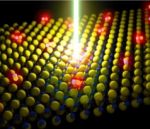
An emerging class of atomically thin materials known as monolayer semiconductors has generated a great deal of buzz in the world of materials science. Monolayers hold promise in the development of transparent LED displays, ultra-high efficiency solar cells, photo detectors and nanoscale transistors. Their downside? The films are notoriously riddled with defects, killing their performance.
But now a research team, led by engineers at the University of California, Berkeley, and Lawrence Berkeley National Laboratory, has found a simple way to fix these defects through the use of an organic superacid. The chemical treatment led to a dramatic 100-fold increase in the material's photoluminescence quantum yield, a ratio describing the amount of light generated by the material versus the amount of energy put in. The greater the emission of light, the higher the quantum yield and the better the material quality.
The researchers enhanced the quantum yield for molybdenum disulfide, or MoS2, from less than 1 percent up to 100 percent by dipping the material into a superacid called bistriflimide, or TFSI.
Their findings, to be published in the Nov. 27 issue of Science, opens the door to the practical application of monolayer materials, such as MoS2, in optoelectronic devices and high-performance transistors. MoS2 is a mere seven-tenths of a nanometer thick. For comparison, a strand of human DNA is 2.5 nanometers in diameter.
"Traditionally, the thinner the material, the more sensitive it is to defects," said principal investigator Ali Javey, UC Berkeley professor of electrical engineering and computer sciences and a faculty scientist at Berkeley Lab. "This study presents the first demonstration of an optoelectronically perfect monolayer, which previously had been unheard of in a material this thin."
The researchers looked to superacids because, by definition, they are solutions with a propensity to "give" protons, often in the form of hydrogen atoms, to other substances. This chemical reaction, called protonation, has the effect of filling in for the missing atoms at the site of defects as well as removing unwanted contaminants stuck on the surface, the researchers said.
Co-lead authors of the paper are UC Berkeley Ph.D. student Matin Amani, visiting Ph.D. student Der-Hsien Lien and postdoctoral fellow Daisuke Kiriya.
Page 1 of 2
Share on:


Testimonial
"Advertising in PCB007 Magazine has been a great way to showcase our bare board testers to the right audience. The I-Connect007 team makes the process smooth and professional. We’re proud to be featured in such a trusted publication."
Klaus Koziol - atgSuggested Items
Curing and Verification in PCB Shadow Areas
09/17/2025 | Doug Katze, DymaxDesign engineers know a simple truth that often complicates electronics manufacturing: Light doesn’t go around corners. In densely populated PCBs, adhesives and coatings often fail to fully cure in shadowed regions created by tall ICs, connectors, relays, and tight housings.
Marcy’s Musings: Advancing the Advanced Materials Discussion
09/17/2025 | Marcy LaRont -- Column: Marcy's MusingsAs the industry’s most trusted global source of original content about the electronics supply chain, we continually ask you about your concerns, what you care about, and what you most want to learn about. Your responses are insightful and valuable. Thank you for caring enough to provide useful feedback and engage in dialogue.
September 2025 PCB007 Magazine: The Future of Advanced Materials
09/16/2025 | I-Connect007 Editorial TeamMoore’s Law is no more, and the advanced material solutions being developed to grapple with this reality are surprising, stunning, and perhaps a bit daunting. Buckle up for a dive into advanced materials and a glimpse into the next chapters of electronics manufacturing.
I-Connect007 Launches Advanced Electronics Packaging Digest
09/15/2025 | I-Connect007I-Connect007 is pleased to announce the launch of Advanced Electronics Packaging Digest (AEPD), a new monthly digital newsletter dedicated to one of the most critical and rapidly evolving areas of electronics manufacturing: advanced packaging at the interconnect level.
Panasonic Industry will Double the Production Capacity of MEGTRON Multi-layer Circuit Board Materials Over the Next Five Years
09/15/2025 | Panasonic Industry Co., Ltd.Panasonic Industry Co., Ltd., a Panasonic Group company, announced plans for a major expansion of its global production capacity for MEGTRON multi-layer circuit board materials today. The company plans to double its production over the next five years to meet growing demand in the AI server and ICT infrastructure markets.